Switch OLED teardown V1/V2

mvmiranda

Well-Known Member
Member
Joined
Oct 29, 2013
Messages
1,457
Trophies
1
Location
Brazil, Sao Paulo
Website
www.gamemod.com.br
XP
1,673
Country
Brazil
The two pins you mentioned are not connected inside the eMMC but the pins on the board could be connected to ground.
So bridging them COULD cause issues in DAT0 touches them.
We need to wait for a proper PCB delayer to see that is connected to where.
THAT could be a thing, yes! :)
 
  • Like
Reactions: sean222

sean222

Well-Known Member
Newcomer
Joined
Sep 7, 2007
Messages
92
Trophies
1
XP
771
Country
Canada
The two pins you mentioned are not connected inside the eMMC but the pins on the board could be connected to ground.
So bridging them COULD cause issues in DAT0 touches them.
We need to wait for a proper PCB delayer to see that is connected to where.
Didn't know this...Thanks!
 

TheUnknownOne

Well-Known Member
Newcomer
Joined
May 29, 2021
Messages
86
Trophies
0
Age
37
XP
333
Country
United States
In the end either we will need to remove, reball and reflow that chip, or some sort of thin PCB that can slide under will be needed.

For those that can't do this type of thing, they will he paying $$$ for the installation alone.
 
  • Like
Reactions: mvmiranda

FR0ZN

Well-Known Member
Member
Joined
Nov 2, 2013
Messages
1,378
Trophies
1
Age
37
XP
3,864
Country
United States
So I was looking at the delayered images of the Switch Lite PCB here: http://balika011.hu/switch/lite/

If you remove the first layer, you get this view:
1635425196601.png

And if you remove 2 more layers you can see this:
1635425284036.png

So to me it seems, that the first layer, is connected to 19 points on the third layer.
If we translate these pins to the top layer, we can see which of these points are connected:

1635425517856.png

So I had a bit of free time and doodled a QSB, which is looks something like this:

1635425995331.png

The idea goes like this:

1) Remove the eMMC and clean it
2) Clean the Switch PCB
3) Solder the QSB to the 19 points on the Switch PCB
4) Use thin double sided tape and apply it to the Switch PCB
5) Flip over the eMMC, so the BGA points upwards and place it face down on the double sided tape
6) Bend the QSB over towards the BGA
7) Solder the QSB onto the BGA and restore the connection to the Switch PCB this way
8) Use exposed DAT0 to solder it to the modchip

So if you'd look at it from the side, it would look like this:

1635426833226.png

NOTE: The design has a few errors on the bottom part - I mirrored it incorrectly and the pin on the bottom needs to be rerouted to the corresponding pin on the BGA.
I just couldn't be assed to finish it 100% in Paint.net, but you should get the idea :D

As I said, this is just me talking out of my ass, but should it be possible to create such a QSB, then I'm sure that this will be a lot easier to install.
Because reworking a BGA, even that small, is not as easy as it seems - but removing the eMMC, cleaning it and soldering 19-20 pins on both sides should be as hard/easy as soldering the SoC QSB.

What do you guys think?
 
Last edited by FR0ZN,

grubgrub

Well-Known Member
OP
Member
Joined
Jun 14, 2015
Messages
333
Trophies
0
Age
44
XP
1,550
Country
New Zealand
So I was looking at the delayered images of the Switch Lite PCB here: http://balika011.hu/switch/lite/

If you remove the first layer, you get this view:

And if you remove 2 more layers you can see this:

So to me it seems, that the first layer, is connected to 19 points on the third layer.
If we translate these pins to the top layer, we can see which of these points are connected:


So I had a bit of free time and doodled a QSB, which is looks something like this:


The idea goes like this:

1) Remove the eMMC and clean it
2) Clean the Switch PCB
3) Solder the QSB to the 19 points on the Switch PCB
4) Use thin double sided tape and apply it to the Switch PCB
5) Flip over the eMMC, so the BGA points upwards and place it face down on the double sided tape
6) Bend the QSB over towards the BGA
7) Solder the QSB onto the BGA and restore the connection to the Switch PCB this way
8) Use exposed DAT0 to solder it to the modchip

So if you'd look at it from the side, it would look like this:


NOTE: The design has a few errors on the bottom part - I mirrored it incorrectly and the pin on the bottom needs to be rerouted to the corresponding pin on the BGA.
I just couldn't be assed to finish it 100% in Paint.net, but you should get the idea :D

As I said, this is just me talking out of my ass, but should it be possible to create such a QSB, then I'm sure that this will be a lot easier to install.
Because reworking a BGA, even that small, is not as easy as it seems - but removing the eMMC, cleaning it and soldering 19-20 pins on both sides should be as hard/easy as soldering the SoC QSB.

What do you guys think?


What about all the other points on the PCB?
Are they not connected to anything?
 

FR0ZN

Well-Known Member
Member
Joined
Nov 2, 2013
Messages
1,378
Trophies
1
Age
37
XP
3,864
Country
United States
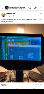
I just saw that the iPhone scene already did what I proposed above.
This has to be the way for people who cant'/don't want to reball.
This method is way safer then the current implementation.
 

Attachments

  • IMG-20211028-WA0017.jpg
    IMG-20211028-WA0017.jpg
    70 KB · Views: 146
  • IMG-20211028-WA0018.jpg
    IMG-20211028-WA0018.jpg
    85.9 KB · Views: 147

mvmiranda

Well-Known Member
Member
Joined
Oct 29, 2013
Messages
1,457
Trophies
1
Location
Brazil, Sao Paulo
Website
www.gamemod.com.br
XP
1,673
Country
Brazil
I just saw that the iPhone scene already did what I proposed above.
This has to be the way for people who cant'/don't want to reball.
This method is way safer then the current implementation.
Riiight!
So, expect it Soon™.

Honestly I was considering your proposal kind of "otherworldly" and then you come and BAM show me something similar already done. :P

Nice! :)
 

FR0ZN

Well-Known Member
Member
Joined
Nov 2, 2013
Messages
1,378
Trophies
1
Age
37
XP
3,864
Country
United States
Riiight!
So, expect it Soon™.

Honestly I was considering your proposal kind of "otherworldly" and then you come and BAM show me something similar already done. :P

Nice! :)
It's not as otherwordly as reworking the BGA while fiddling a cable in there :D

I also just noticed that they can grab all other signals from there as well (CLK, CMD, etc.)

So this way the install could consist of 2 QSBs just like the Lite + is cleaner + safer.
I realy hope they do it this way.
 
  • Like
Reactions: mvmiranda

FR0ZN

Well-Known Member
Member
Joined
Nov 2, 2013
Messages
1,378
Trophies
1
Age
37
XP
3,864
Country
United States
@FR0ZN, any good news? Seems no such cable anybody used for oled switch.
Hope someone have a try and success!
I haven't looked further into this.
As I said, I never made any PCB designes myself - what I showed was just me doodleing something together :D

I myself am currently putting my hopes into whoever is building the HWFLY modchips, to create a redesign for the OLEDs and adapt the eMMC flex cable method.

Slaughtering a Core or Lite modchip into the OLED is "dirty" imo.
 
  • Like
Reactions: mvmiranda

vailon_yg

Member
Newcomer
Joined
Oct 24, 2021
Messages
11
Trophies
0
Age
42
XP
119
Country
China
I haven't looked further into this.
As I said, I never made any PCB designes myself - what I showed was just me doodleing something together :D

I myself am currently putting my hopes into whoever is building the HWFLY modchips, to create a redesign for the OLEDs and adapt the eMMC flex cable method.

Slaughtering a Core or Lite modchip into the OLED is "dirty" imo.
That's a good idea~~
 
  • Like
Reactions: mvmiranda

Site & Scene News

Popular threads in this forum

General chit-chat
Help Users
    K3Nv2 @ K3Nv2: They really wanna get the head