- Joined
- Jul 20, 2019
- Messages
- 94
- Trophies
- 0
- Age
- 34
- Location
- Around the world
- Website
- www.google.com
- XP
- 196
- Country

Ive started to do an experiment, I want to work out how some parts of the PCB connect to each other so we can build some rudimentary schematics.
I have 1 board.. HAC-CPU-10 (CW) that has given me all I needed.. it has been a really nice donor and although it still have some chips I can harvest .. and I dont have any more switches to repair because I am awaiting parts... I have decided to start a little project.
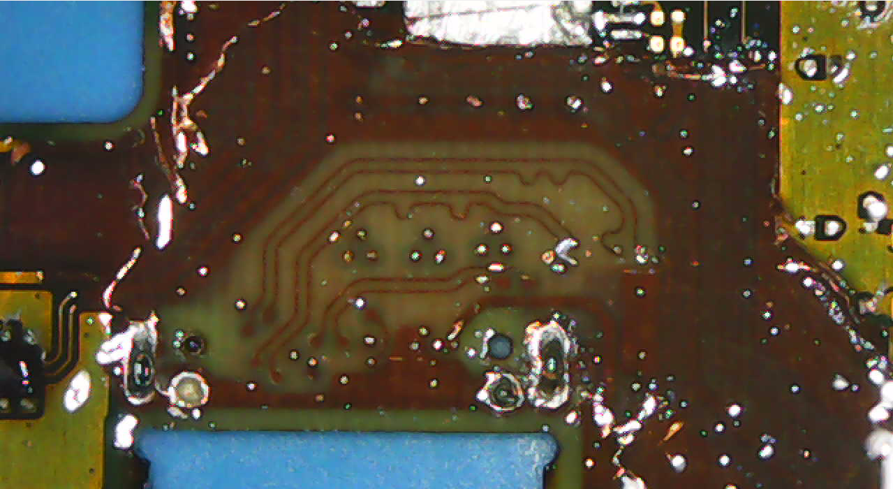
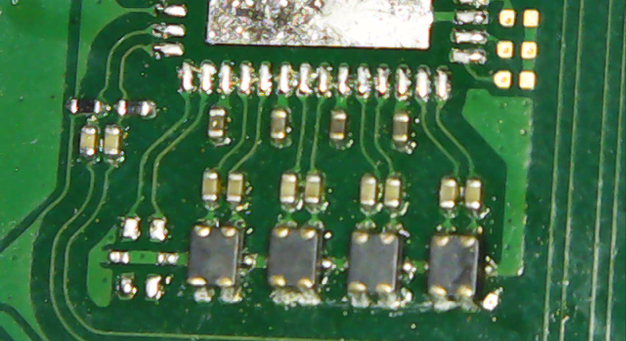
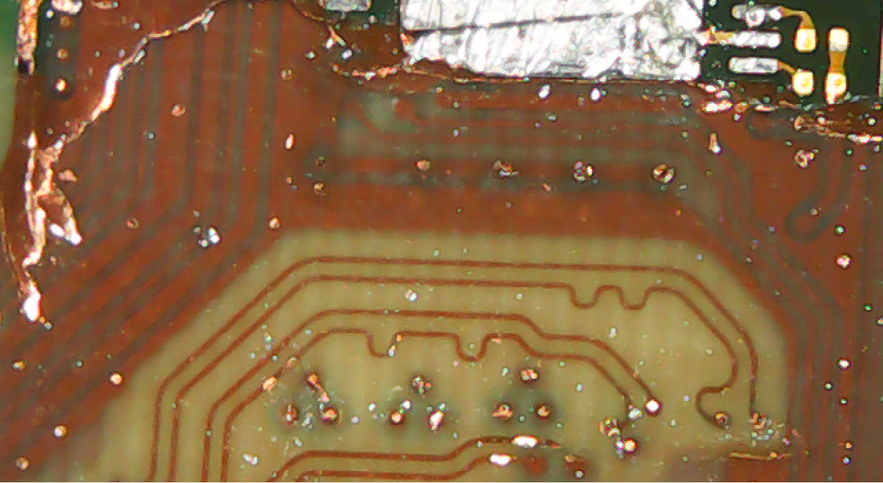
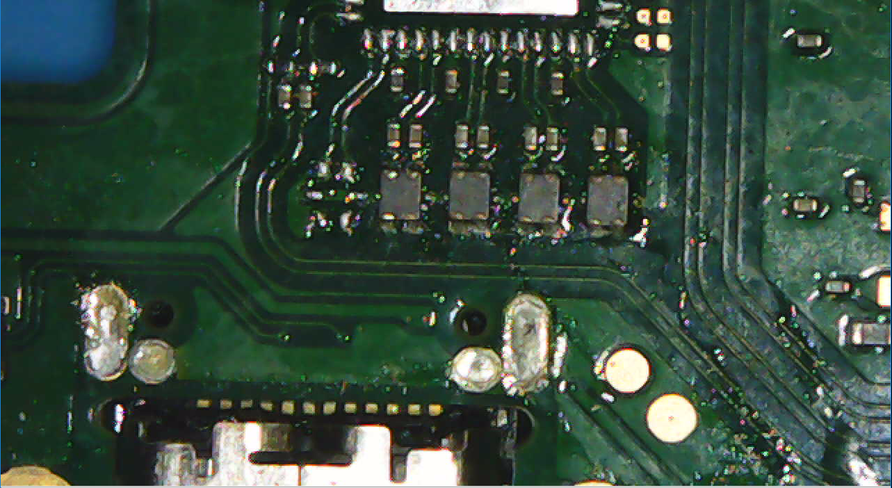
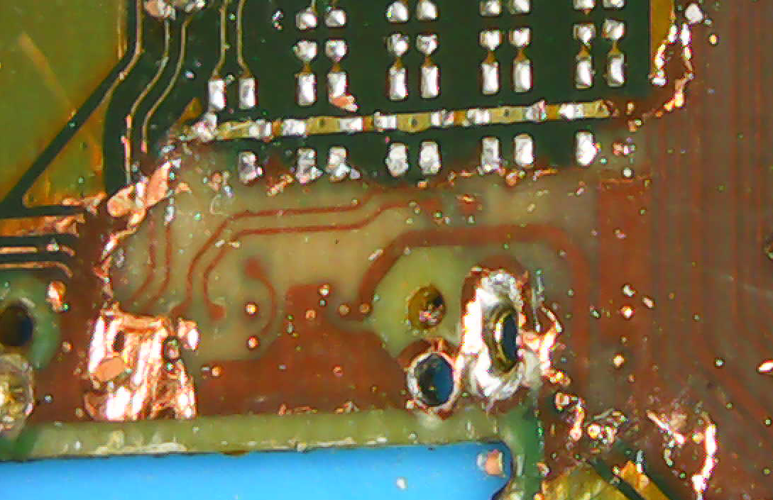
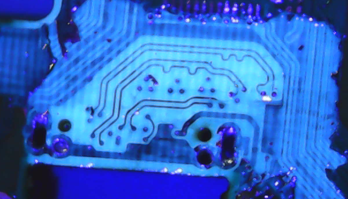
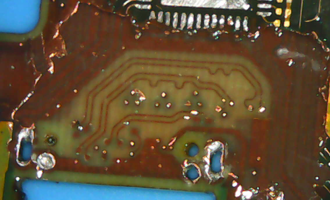
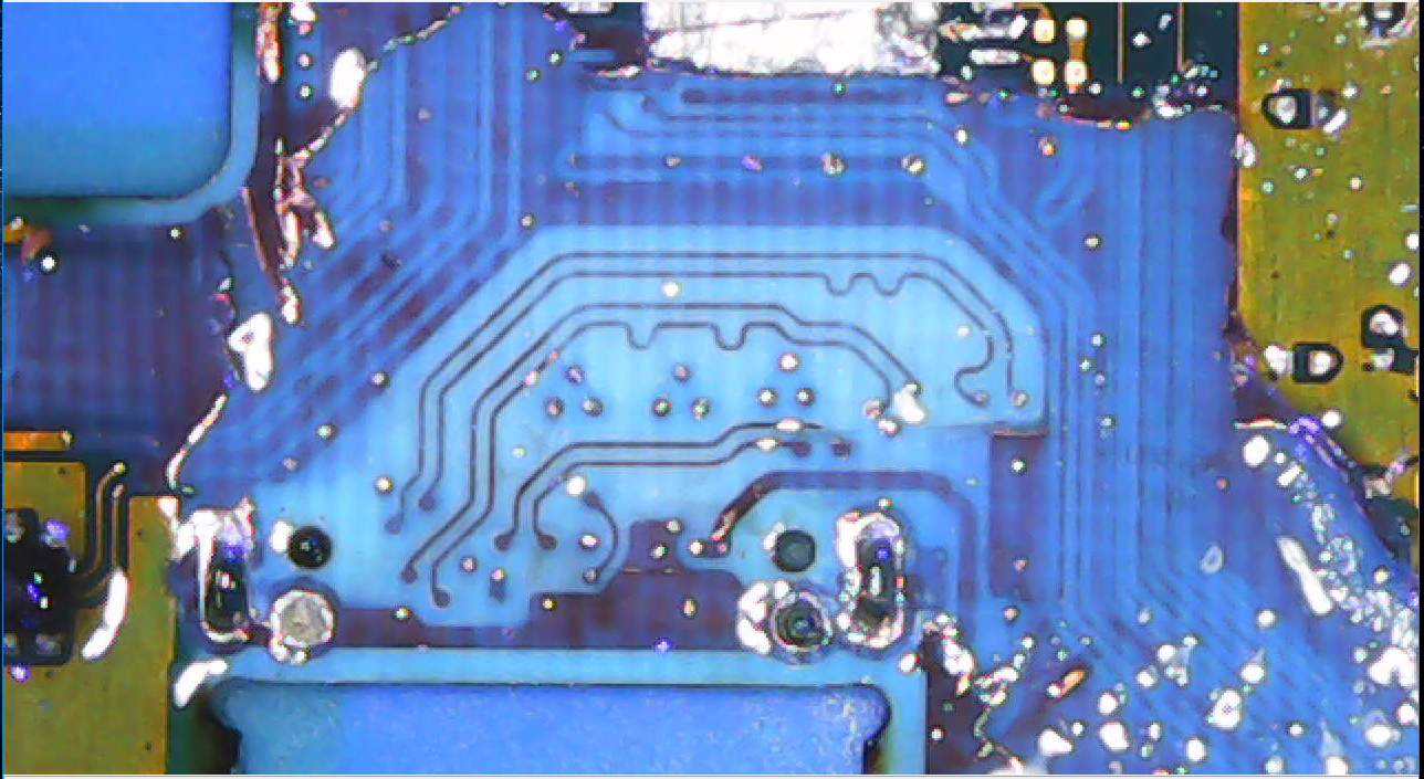
I am going to strip the layers of the PCB bit by bit and I will post images here so that in a near future we can build some schematics with this and some reading.. this thread will be my "blog" somehow.. I will try post images of the layers peeled (my microscope is not too good so sorry for the quality) I will also post images whit the UV lamp to see the traces well.. and also will try to post references from another donor board I have (may not be pretty but is what I have that I can trash..)
Today, I wanted to understand how the PI3USB data lines (DP0, 1, 2 ,3 and Aux) signal go through the chokes to the USB port and which pins are used to communicate here.. Also those I/O lines.
I want people to debate, I want to hear loads of opinions and comments so please go ahead, this is an open forum to discuss how this PCB is built and draw some conclusions
also I want guidance.. what would you do next?


