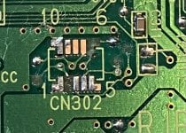
The red circled area, used to be a pad there ("D" on the second image). This is for the Xeno chip mod. I'm gonna try one of the alternate points, but just wondering if I might need to do the alternate method on the backside of the PCB.

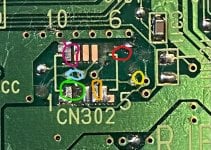
Thanks, here is a picture I found of alternate points that I was trying out:GC stuff at this level is not my forte such that I know alt pins off the top of my head.
That said simple visual observation has that it looks like a simple test pad not connected to anything beyond it. To that end you have the remains the of the trace, the via and what at this point is your most likely target in the little pad next to the other lead you have there/above the n on the mask/that is also tinned in the picture with the mod chip, plus if push comes to shove wherever that via winds up coming out.
Alternatively figure out what the pin on the chip is doing and find a replacement for that (hopefully it is something boring and basic like voltage source or ground, I can't tell what it is connected to from the picture though).
The pad you ripped off is a testpoint - it shouldn't affect operation. Just solder the wire either to the pad for pin 2 (next to the blue wire in your photo) or to the via.
If I were you I would do some reflowing on those wire points, they look pretty jank and could cause cold (broken) joints. A contact point that you are soldering should flow naturally and look smooth, anything like that might have uncertainty with consistent or proper bonding.
Also what kind of gauge wire are you using with this?
Use flux
I did not know you had troubled the chip. In that case looking at that picture 4 and the xeno gc part under 5 appear to be connected via the 102 (in surface mount stuff that means 10 and 2 0's https://www.instructables.com/Reading-Surface-Mount-Resistor-codes/ ) in presumably a pull down/pull up arrangement. You might need to replicate that.
I also can't see 3 on that but what is there has the telltale brown of a lifted pad for part of that.
I also don't like the look of the connection of the brown I am guessing that is a ferrite bead but might be a capacitor across from 3 on that.
Ferrite beads are available in many places -- they are weak inductors usually there to stop noise. You might even find it works if you bridge it out as noise might only be present in certain models of GC or setups.
If it is a capacitor then hopefully there are some numbers as you want to know what it is before you start messing with replacements.
Soldering to vias and traces is a pain. Scrape it a bit with a scalpel if you can.
To be honest, all that stuff is way beyond my current skill level. I might just be better off getting a replacement PCB and trying again with the traditional wired install. Before doing that though I might try the backside of the PCB even though that's working with significantly smaller components. Who knows though, maybe I can get it to work without needing to go that route.
Also I just wanted to say thanks so much for all your input, super helpful stuff. Posts like yours are why I love this community so much.
The brown component to the left of the MCU is a decoupling capacitor and it's wired directly across the power line - the pad you have marked as "4" (I.E. power) goes to the top of it and the one you have marked as 6 (I.E. Ground) goes to the bottom - you can just solder the wires directly across the cap. You want to be a little careful to avoid overheating the cap too much.
") SO happy right now that I managed to get everything to work! Thanks again everyone for all the help and encouragement
SO happy right now that I managed to get everything to work! Thanks again everyone for all the help and encouragement 
OK, looks like you worked it out - basically you have lost enough of the pads that you need to solder the wires to the vias, For future reference, thinner wires would be a good idea because they reduce the risk of ripping the pads off.

Yup, I finally realized that was pretty much my only option. I actually learned quite a bit about soldering doing this- although I definitely wouldn't recommend it as someone's first or second-ever project (it as my second)
Good suggestion about the wires! Yeah 24 AWG is too thick I think for this kind of work.
I've always regarded QSBs as being something of a trap for the inexperienced. Yes, they allow you to connect things quickly if you have a fair bit of soldering practice, but they are also very easy to mess up and quite hard to remove cleanly if you aren't so experienced with soldering.
I've seen this quite a bit recently with Xstation for the PSX - people tend to assume that because it's using a QSB it's a good beginner project and end up damaging the QSB the mainboard or both.
Just curious, is a modchip for gc still worth getting when the ode gc loader pnp exist?
GC Loader is arguably the best solution and more future-proof than the aging optical drives.Just curious, is a modchip for gc still worth getting when the ode gc loader pnp exist?
Soldering must be practiced – like everything. Using good flux is gonna help a lot (I didn't want to believe it at first since most solder comes with a bit of flux inside). Gain some confidence with practice boards or with scrap electronics. Everybody can do basic soldering – I can do it with my movement disorders (shaking hands).I can attest to the easy to mess things up part! In hindsight I would have at least got some cheap practice boards from Amazon or something to try and learn the basics before diving in headfirst.
Soldering must be practiced – like everything. Using good flux is gonna help a lot (I didn't want to believe it at first since most solder comes with a bit of flux inside). Gain some confidence with practice boards or with scrap electronics. Everybody can do basic soldering – I can do it with my movement disorders (shaking hands).