Hacking 3DS unbricking progress

  • Thread starter Thread starter krisztian1997
  • Start date Start date
  • Views Views 376,676
  • Replies Replies 1,233
  • Likes Likes 32
Status
Not open for further replies.
What switch? XD the arduino Works with 5v signal levels wich would kill the Sd and the resistor voltage dropper does the Job unsafely. Thats why the logic level shifter is mandatory. You put 3.3v to the ref pin (vcc) then all signals on the A pins are converted down to a stable 3.3v and a stable current onthe B pins

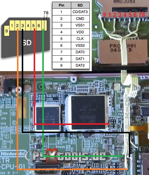
have a look at the middle picture in http://gbatemp.net/threads/3ds-unbricking-progress.361171/page-16#post-4904962 . i just wanted to make sure if that swirtch toggled input or output voltage, as i belive it's used to set the input (so the shield can also be used with 3.3V logic microcontrollers by skipping the conversion)
 
k

Moquedami could you give a link for the shield you are using or it's name? not that you fry your 3DS

Hi Bkifft!
This is the shiled I´ve got:
lector-de-tarjetas-sd-micro-sd-spi-arduino-arm-pic-4203-MLA2899967966_072012-O.jpg

lector-de-tarjetas-sd-micro-sd-spi-arduino-arm-pic-4184-MLA2899968016_072012-O.jpg

lector-de-tarjetas-sd-micro-sd-spi-arduino-arm-pic-4244-MLA2899968114_072012-O.jpg

The description goes " Card reader SD MicroSD SPI Arduino Arm pic"
It doesn`t have a brand, model whatsoever. seems the generic type they sell in Dealextreme.
 
What switch? XD the arduino Works with 5v signal levels wich would kill the Sd and the resistor voltage dropper does the Job unsafely. Thats why the logic level shifter is mandatory. You put 3.3v to the ref pin (vcc) then all signals on the A pins are converted down to a stable 3.3v and a stable current onthe B pins

This is the switch we talk about:
24l7sly.jpg
 
I find it wierd that the DAT0 and GND seem inverted between the SD card and the shield.

In the card / In the shield
BLACK - DAT3 / BLACK - SC
BLUE - CMD / BLUE - DI
RED - CLK / RED - CLK
PURPLE - GND / GREEN - DO
GREEN - DAT0 / PURPLE - G
 
Let´s make this as stupidproof as possible.
So I connect the "+" in the shield in this pin and we are all set:
fwrod5.jpg

What about the inverted GND - DAT0, isn´t that strange?


* sorry about the picture-galore. I´m trying to make this as graphic as possible and then I´ll use this to make an easy guide for other people.
 
Let´s make this as stupidproof as possible.
So I connect the "+" in the shield in this pin and we are all set:

What about the inverted GND - DAT0, isn´t that strange?


* sorry about the picture-galore. I´m trying to make this as graphic as possible and then I´ll use this to make an easy guide for other people.

I dont think that the GND is inversed with DAT0, try the shield with a cheap SD card first
 
This is what I mean. When the SD is inserted those connections don´t seem to correlate correctly

1zzm2a0.jpg
 
Guys, is this too small of a connector?
14kfaet.jpg

5 pins, adrino requires a 5th correct?
if i do 5 pins will i still be able to do raspberry pi unbrick also?
 
Guys, is this too small of a connector?
[pic removed]
5 pins, adrino requires a 5th correct?
if i do 5 pins will i still be able to do raspberry pi unbrick also?

the connector size doesn't matter at all as long as you are comfortable with installing it. We are cooking with about 100mA (and thats vor the supply voltage, not the data lines which should draw way less amp) here and i'm not aware of any physical connector that cant handle that.

and yes, the extra connection doesn't matter for raspberry or sd readers
 
DAT0
DAT3
CMD
CLK
GROUND

Ive seen ground connected to two places, the blob of solder shown below and then somewhere over the NAND chip, does it matter?

Nope, it doesnt matters, some connect it to a pin next to the NAND but the cart slot is also good for GND
 
  • Like
Reactions: Habbert
The communication between the card and the 3DS is almost the same like the SD communication, I am not an expert myself but I dont think that the 3DS can reprogram the FPGA, but maybe they will update it in a different way.

If you check my previous thread on the matter, people linked to the data sheet for the Pro ASIC 3 chip, which stated that the JTAG pins were the only way to update the FPGA.
So, if that's indeed the case, how else can one update it? I'm asking because on Gateways website, they state that the upcoming 2.0 Final will have a FPGA update, so I'd like to know what they're talking about (and how they can accomplish it, when a few people are saying its not possible).
 
That switch is supply voltage but will look further if it's the Sd card or the logic level shifter. But i Think it is to what voltage the IC is changing to then it shall be 3.3V

Edit: might be talking out of my hat as im not at Home atm xD working
 
Status
Not open for further replies.

Site & Scene News

Popular threads in this forum