Hardware How I fixed 160-0103 system memory error

Voultar

Well-Known Member
Newcomer
Joined
Nov 1, 2021
Messages
59
Trophies
0
Age
44
XP
322
Country
United States
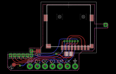
Would it not be possible to make the PCB a little shorter to clear U29 entirely? For example (And please forgive my terrible photo editing skills)

<EDIT> If the issue is clearance for inserting/removing the microSD card, would it fit better if the slot was rotated 180degrees? Something closer to the attached mockup, although obviously the traces would need rerouting,

Or alternatively there are 'flip top' micro SD slots which wouldn't require the extra space for insertion/removal.

No, I'm not compromising the integrity of the memory by using an unreliable interconnect. Those "clam-shell' SD card sockets are terribly unreliable. I'm only going to use a spring mechanism, self locking interface as this is designed to install once and never touch again.

It's fine the way that it is, currently. But if you can source a micro SD connector that's both shallow and not a piece of shit, I'll consider it.

There's no point into going to all of this trouble and then use an unreliable, questionable interface for a system that already has memory problems.
 
Last edited by Voultar,

Razor83

Well-Known Member
Member
Joined
Dec 23, 2009
Messages
391
Trophies
1
XP
1,758
Country
No, I'm not compromising the integrity of the memory by using an unreliable interconnect. Those "clam-shell' SD card sockets are terribly unreliable. I'm only going to use a spring mechanism, self locking interface as this is designed to install once and never touch again.

It's fine the way that it is, currently. But if you can source a micro SD connector that's both shallow and not a piece of shit, I'll consider it.

There's no point into going to all of this trouble and then use an unreliable, questionable interface for a system that already has memory problems.
Sorry I was only trying to help with suggestions :(

Would the currently selected microSD slot give better clearance if it was rotated 180degrees?
 
Last edited by Razor83,

Razor83

Well-Known Member
Member
Joined
Dec 23, 2009
Messages
391
Trophies
1
XP
1,758
Country
I'm thinking omitting the dampening resistors from the PCB and using what's already on the Wii-U.
I think simply flipping the micro SD slot would work perfectly, it should even allow the dampening resistors to fit and require even fewer vias, since you can just connect the pin header vias to the resistor vias directly. It would also help reduce the board size enough to avoid U29.

Please dont take my posts as any criticism of the current design - its already really nice and I only wanted to help make it the best it can be.
Wii U PCB Mockup.png
 
Last edited by Razor83,

SDIO

Well-Known Member
OP
Member
Joined
Feb 13, 2023
Messages
1,973
Trophies
0
Age
28
XP
1,266
Country
Germany
I am also wondering what's the reason for having the SD slot rotated that way.

I also had these thoughts:
If you would also ways connect the SD clk with the Wii U. If someone wants to disable the SD, he still can do so by simply removing it. But with that you would remove the easy "switch between" option which could give users wrong ideas.
Maybe make the jumper for switching the emmcs clk source between PC and Wii U. And maybe also give an option to ground the emmc clk.

For someone who doesn't want to cut the trace and can still run a software dumper I would also see the option to just remove the CMD resistor. Then it wouldn't matter if the eMMC gets a clock. As long as it doesn't receive CMD 1 it shouldn't do anything. But for hardware dumping the eMMC it would still require cutting the clk trace.

If I understand correctly this board would solder to the pads of the resistors, wich is probably the cleanest solution. But I could see people accidentally desoldering the resistors or bridging them. Maybe it would be easier to solder to the nearby VIAs. Any thoughts on that?

To get rid of that one cable for the 3V3 supply I could see the option to add a linear voltage regulator to the qsb and getting 5V from the cap near by. But that's just a thought and I believe getting the 3V3 that is already there with a cable is the better option

Do you know what type of component Q6 is?
 

Razor83

Well-Known Member
Member
Joined
Dec 23, 2009
Messages
391
Trophies
1
XP
1,758
Country
If I understand correctly this board would solder to the pads of the resistors, wich is probably the cleanest solution. But I could see people accidentally desoldering the resistors or bridging them. Maybe it would be easier to solder to the nearby VIAs. Any thoughts on that?
Yes I had wondered about potentially soldering to the via's too. However i'm not sure if the Wii U has tented vias? In which case people would have to scrape away the solder mask, which might be beyond some peoples skill/comfort level.

Also looking at the back of the Wii U motherboard there is quite a bit of free space if we could potentially solder to the vias. Although it would probably make it more difficult to connect up a pin header to read the eMMC, and I dont think there is any access to both sides of the CLK signal (R26) from the bottom side of the board.

Overall its probably easiest to use the resistors as the connection points as they should also make a nice anchor point for the board. My only concern is the risk of people knocking the resistors off when soldering, although really once the eMMC has been dumped it shouldn't really matter if they are accidentally removed.
 
Last edited by Razor83,

martindrengen

Member
Newcomer
Joined
Jul 21, 2020
Messages
20
Trophies
0
Age
36
XP
154
Country
Denmark
This will not lay perfectly fat. The edge of the board will rest on components at an angle.

The PCB thickness will be between .6mm and 1mm to accomodate for just a little bit of flex.

I think @Razor83 has a lot of good suggestions. It would be much better if the board was able to lay flat. You mention board flex, does that imply that there will be strain on the solder pads? It may not be an issue right away but continued strain on resistors possibly could lead to them cracking with time.
 

V10lator

Well-Known Member
Member
Joined
Apr 21, 2019
Messages
2,585
Trophies
1
Age
36
XP
5,366
Country
Germany
Do we really need to have "Wii-U NAND" or "Wii-U NAND REBUILDER" written on it? I think just removing that print would save a lot of space, which IMO is a good thing, too.
 

Razor83

Well-Known Member
Member
Joined
Dec 23, 2009
Messages
391
Trophies
1
XP
1,758
Country
@SDIO Do you know if there is any app on the Wii U which can report the eMMC chips hardware and firmware revisions? I recently saw that nyx on the Switch can show these details, and thought it would be nice if we could get a clearer picture of exactly which Wii U eMMC chip hardware/firmware revisions have the most failures:-
nyx20230326_151231-png.360843
 

SDIO

Well-Known Member
OP
Member
Joined
Feb 13, 2023
Messages
1,973
Trophies
0
Age
28
XP
1,266
Country
Germany
In
Yes I had wondered about potentially soldering to the via's too. However i'm not sure if the Wii U has tented vias? In which case people would have to scrape away the solder mask, which might be beyond some peoples skill/comfort level.
No the VIAs are not tented, I had no problem soldering to them. At least on my WUP-01 one. I didn't disassemble the others yet.


Also looking at the back of the Wii U motherboard there is quite a bit of free space if we could potentially solder to the vias. Although it would probably make it more difficult to connect up a pin header to read the eMMC, and I dont think there is any access to both sides of the CLK signal (R26) from the bottom side of the board.
I would prefer to keep it on side B (top). To solder to SIDE A, you have to do more disassembling, including removing the heatsink to remove the buttom RF shield. And for reading the eMMC you would have to install the heatsink again, as you need to power on the Wii U.

Overall its probably easiest to use the resistors as the connection points as they should also make a nice anchor point for the board. My only concern is the risk of people knocking the resistors off when soldering
Exactly my thought
although really once the eMMC has been dumped it shouldn't really matter if they are accidentally removed.
If someone wan't to use this board to dump or flash the eMMC, he still needs the resistors.

@SDIO Do you know if there is any app on the Wii U which can report the eMMC chips hardware and firmware revisions?
There ist, it's called mdinfo and I posted a version earlier in the thread that extracts the manufacturing date.
 

Razor83

Well-Known Member
Member
Joined
Dec 23, 2009
Messages
391
Trophies
1
XP
1,758
Country
No the VIAs are not tented, I had no problem soldering to them. At least on my WUP-01 one. I didn't disassemble the others yet.
Well thats good to know, certainly opens up more options.

I would prefer to keep it on side B (top). To solder to SIDE A, you have to do more disassembling, including removing the heatsink to remove the buttom RF shield. And for reading the eMMC you would have to install the heatsink again, as you need to power on the Wii U.
Yeah I agree, it would probably be better and more convenient to keep it on the topside.

If I recall correctly though I dont think you actually have to remove the heatsink to take off the bottom RF shield? The heatsink has to be unscrewed, but you dont actually have to take it off - at least thats what I recall from the last itime I took apart a Wii U some years ago.

Exactly my thought

If someone wan't to use this board to dump or flash the eMMC, he still needs the resistors.
Sure, but I thought it would probably be recommend to attempt a software dump of both the MLC and eMMC using UDPIH before removing power and installing the board? Or would that not be enough to work with the SLC cache?

There ist, it's called mdinfo and I posted a version earlier in the thread that extracts the manufacturing date.
Thanks, mdinfo appears to show the CID and CSD - but do these strings contain the HW and FW revisions of the eMMC?

I'm just really curious to know if one of the causes of the 160-0103 error might actually be a faulty fimware revision on some eMMC chips causing corrupting issues. It has been discovered that faulty eMMC firmware has caused corruption on some devices previously:-


I made a post about this potential cause some years ago here:-
https://gbatemp.net/threads/possibl...rror-code-160-0103.460359/page-3#post-7269430
 
Last edited by Razor83,

Voultar

Well-Known Member
Newcomer
Joined
Nov 1, 2021
Messages
59
Trophies
0
Age
44
XP
322
Country
United States
I'm looking at the datasheets, and I don't believe we need bus termination resistors for use with SD-Cards that we're using to replace busted eNANDS with. I believe we can safely omit these and be problem free.
The I/O is 3V3, the resistors are there to help clamp signals and back terminate them to match the drivers resistance. But in this specific application with the memory that we're replacing it with, it doesn't really matter much.
Just as there are no pull-up resistors to keep a logic state from floating, the SD-Cards that we're using will work and not care.
This will save tremendous space
Post automatically merged:

reworked.jpg


1) Soldering to vias. - Vias are weak and don't make for a strong mechanical bond. They're prone to being damaged and shouldn't be used (especially at this size) unless you really have to. On top of that, most of these boards do have a conformal coating, separate from actual solder resist/tenting. The 0402 resistors will provide a nice, clean mechanical bond and this is ideally where the PCB should be affixed to.

The SD-Card has been rotated and dropped significantly do give clearance to be cycled from the other direction. Of course, c617 isn't populated on any of the 7 systems that i have but it might be on yours.

2) I believe I'm going to omit the SD/EMMC jumper all together. At this point, I don't see the utility of switching between onboard memory and your memory replacement. I see more people disturbing the SLC cache and making their problems much worse by using this jumper and not understanding it so I think it's best to drop it.

However, I WILL add a jumper that will allow you to pull the CLK on the eNAND low (ground) so that it doesn't float and behave erratically.
 
Last edited by Voultar,

SDIO

Well-Known Member
OP
Member
Joined
Feb 13, 2023
Messages
1,973
Trophies
0
Age
28
XP
1,266
Country
Germany
This looks really good now. Maybe you could make it so it can be soldered to one of the pads of the unpopulated cap, so it has more mechanical strength for inserting/removing a sd?

Could signal integrety become a problem, if the only GND connection is to this one electrolytic cap to the right, so the return path for the signals is quite a bit longer or is the frequency (50Mhz) so low that this is not a concern?
 
  • Like
Reactions: Xerczese

V10lator

Well-Known Member
Member
Joined
Apr 21, 2019
Messages
2,585
Trophies
1
Age
36
XP
5,366
Country
Germany
However, I WILL add a jumper that will allow you to pull the CLK on the eNAND low (ground) so that it doesn't float and behave erratically.
When you won't add a jumper to switch between eMMC and SD, why even add a CLK to GND jumper? I mean why not just have CLK always at GND when you completely disable the eMMC anyway?

Also why keep the eMMC dumping pads when there's no way to use the eMMC anymore? For flashing the SD card it would be way more simple to remove it from the board and use a proper card reader on PC.

I think it's a bit sad to remove the SD or eMMC jumper. There will be no way to hardware dump the eMMC this way and experienced people who might want to switch between both for researching will be left in the dark.
 

Voultar

Well-Known Member
Newcomer
Joined
Nov 1, 2021
Messages
59
Trophies
0
Age
44
XP
322
Country
United States
This is
Could signal integrety become a problem, if the only GND connection is to this one electrolytic cap to the right, so the return path for the signals is quite a bit longer or is the frequency (50Mhz) so low that this is not a concern?

The ground connection is very large and rigid. Both top and bottom layers of this PCB have been filled with ground-plane so at bandwidth that this SD-Card switches across, it's more than sufficient.
 

Attachments

  • Wii-U NAND-AID.png
    Wii-U NAND-AID.png
    103.3 KB · Views: 32

SDIO

Well-Known Member
OP
Member
Joined
Feb 13, 2023
Messages
1,973
Trophies
0
Age
28
XP
1,266
Country
Germany
Also why keep the eMMC dumping pads when there's no way to use the eMMC anymore? For flashing the SD card it would be way more simple to remove it from the board and use a proper card reader on PC.
I think the eMMC clk is the one exposed on the header. So basically the eMMC is permanently connected to the dumping header and the SD permanently to the Wii U
 

Voultar

Well-Known Member
Newcomer
Joined
Nov 1, 2021
Messages
59
Trophies
0
Age
44
XP
322
Country
United States
When you won't add a jumper to switch between eMMC and SD, why even add a CLK to GND jumper? I mean why not just have CLK always at GND when you completely disable the eMMC anyway?

Also why keep the eMMC dumping pads when there's no way to use the eMMC anymore? For flashing the SD card it would be way more simple to remove it from the board and use a proper card reader on PC.

I think it's a bit sad to remove the SD or eMMC jumper. There will be no way to hardware dump the eMMC this way and experienced people who might want to switch between both for researching will be left in the dark.
That isn't how that works.

If you look at the footprint for the EMMC breakout points at the bottom, the CLK signal from the EMMC, not the Wii-U goes there and only there. The jumper wasn't responsible for allowing you to dump the original eMMC, it was only going to allow you to boot the Wii-U with either the original eMMC or the replacement.

The new PCB (see pictures) has a jumper that allows you to short the CLK of the eMMC to ground when closed so that its logic state isn't floating. If you keep this jumper open, you can read the eMMC memory, just as you could before. You'll want to short it after you've dumped the memory so that it won't try to fight on the bus with the SD replacement as it's input (CLK) would be floating around.

I may put a castellated edge below the 3V3 power pad to grab another ground for anchor.
 

SDIO

Well-Known Member
OP
Member
Joined
Feb 13, 2023
Messages
1,973
Trophies
0
Age
28
XP
1,266
Country
Germany
The ground connection is very large and rigid. Both top and bottom layers of this PCB have been filled with ground-plane so at bandwidth that this SD-Card switches across, it's more than sufficient.
But if I see it correctly there is no GND connection near the connection for the Signals. So the return path for the signals is first to the right. then then probably through a GND layer in the mainboard. So the loop area is much bigger. The ground fill of the QSB won't help with that, as there is no GND connection on the left.

But also I don't see a good point to get a GND connection near to the resistors, except some VIAs and it will probably work as it is.
Post automatically merged:

You'll want to short it after you've dumped the memory so that it won't try to fight on the bus with the SD replacement as it's input (CLK) would be floating around.
I agree that it's good practice to not have inputs floating and I also recommend grounding it. But I am not that concerned that it will cause a bus conflict. The eMMC shouldn't drive the bus without either first receiving CMD1 or if the eMMC enters boot mode by holding CMD low for 74 and more clock cycles after power up (if it sees CMD high at any point it will leave boot mode).
I think it's very unlikely that the eMMC sees any of this by accident.
 
Last edited by SDIO,

Voultar

Well-Known Member
Newcomer
Joined
Nov 1, 2021
Messages
59
Trophies
0
Age
44
XP
322
Country
United States
How are people interfacing these eMMCs to their PCs? I'm sure they're using an SD card reader, but are they hacking up an SD-Card to wire these in?

Is there a better option?
 

Site & Scene News

Popular threads in this forum

General chit-chat
Help Users
  • No one is chatting at the moment.
    Sicklyboy @ Sicklyboy: *teleports behind you* "Nothing personnel, kiddo" +1