Hello everyone,
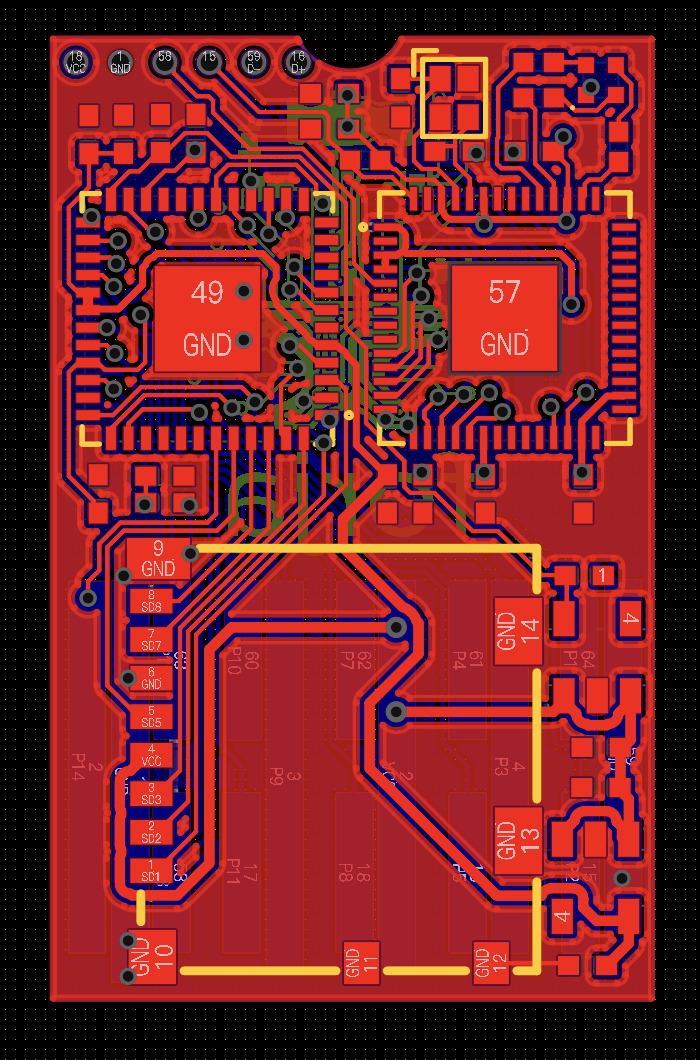
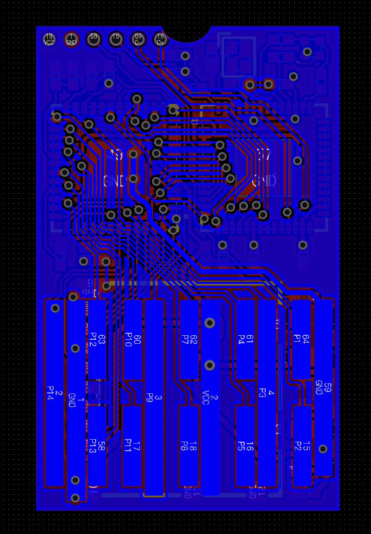
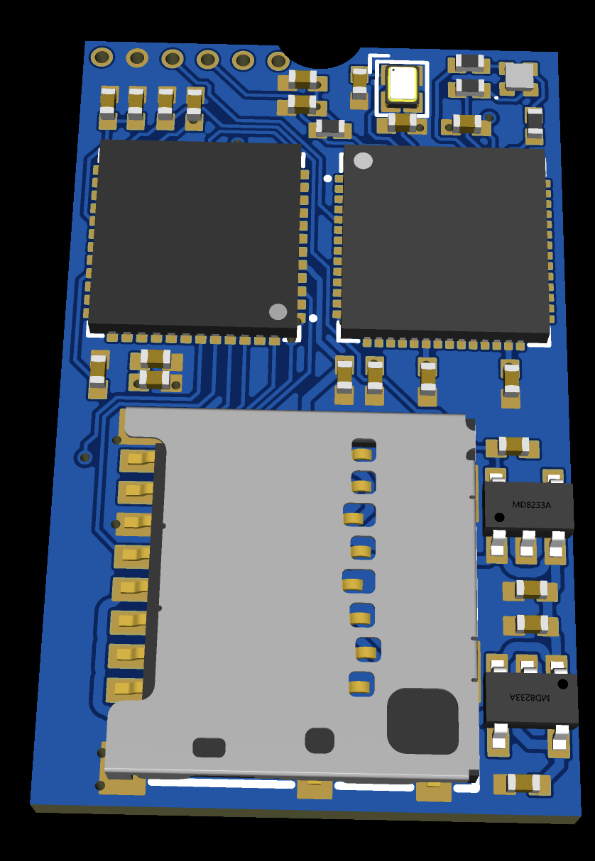
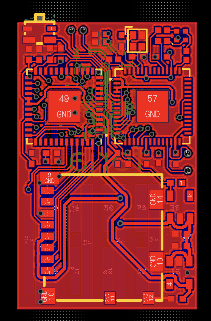
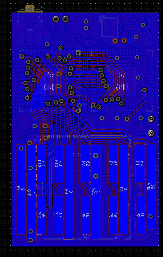
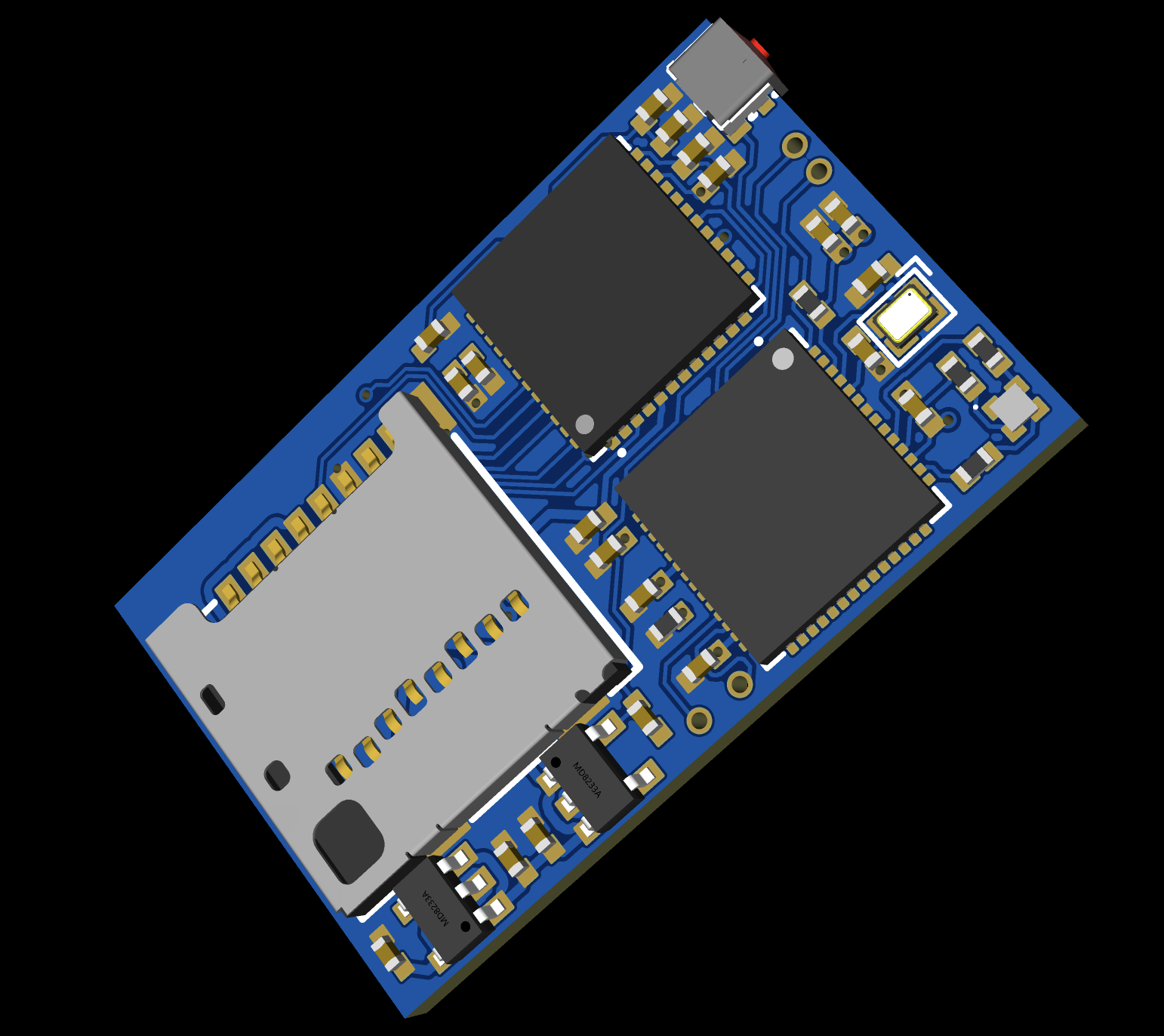
I've been spending some time recently doing a deep dive into the M1gSwitch hardware, and I took a few hours to measure and completely redraw the PCB. After I finished, I discovered that another member of the community had already done the same work, haha.
But since the project is complete, I wanted to share my version and my thoughts on what could be done next.
1. My Replicated PCB Design
My goal was to create a low-cost version, so the design is based on JLC's free prototyping service, using 0402 components to match the original's form factor.
- I've created two versions of the board: one minimalist version without a physical button, and a second version that includes one for switching games.
- I also designed a 3D-printable shell to house the board and protect it.
View attachment 525921View attachment 525922View attachment 525924View attachment 525926View attachment 525927View attachment 525928
2. Theory on the FPGA Firmware
I haven't been able to find any public firmware dumps for the FPGA. However, after analyzing the connections between the ESP32 and the FPGA, I saw that the layout perfectly matches the standard for an FPGA's slave configuration mode.
Combined with the fact that the MigSwitch team has released firmware updates, this leads me to a theory:
The FPGA chip likely arrives blank from the factory. On each power-up, the ESP32 is responsible for loading the firmware directly onto the FPGA.
To test this theory, I've ordered new, blank FPGA chips of the same model. There's a slight shipping delay, but I will post an update here as soon as they arrive and I've had a chance to test them.
3. Offering Help to the Community
I'm based near Shenzhen, which allows me to source a wide variety of electronic components and get PCBs manufactured quickly and at a very low cost.
If anyone in the community has a new concept or needs assistance with hardware validation, I'm happy to help.
4. Next Steps: Side-Channel Analysis
Beyond just verifying the FPGA theory, I have some further plans.
- Development Board: I have already created a custom Switch cartridge-style dev board that breaks out all the key interfaces (Power, JTAG, USB, GPIOs) to make debugging and analysis easier.
- Tools: I'm planning to acquire a good oscilloscope and a ChipWhisperer-Husky for this purpose.
- Goal: My objective is to use this setup to perform side-channel analysis and attempt to extract the firmware via non-invasive methods.
- Promise: If I successfully extract a usable firmware, I will release it publicly for the community.
As a side note, the total hardware cost for this replication project is under
40 RMB (about $5-6 USD), making it very accessible.
5. A Long-Term "Moonshot" Idea
Finally, there's a more ambitious, long-term idea. A friend of mine who works in the semiconductor industry suggested that we could potentially use their lab's
FIB (Focused Ion Beam) and electron microscope to directly read the eFuse data from the chip's die. This is a highly advanced physical attack. Their equipment is in constant use, so this is more of a future possibility than a concrete plan, but it remains an interesting option.