



So start off, i must clear that there's another thread that attemped their own research. But since i (personal view btw) see that there's sadly no to little progress coming along i have decided to restart the research or well update it...
ALSO DISCLAMER: I DON'T (N4A) OWN ANY Tamagotchi Uni DEVICE. NOR BE RESPONSABLE OF THE DAMAGE/GORE OR CONSEUQUENCES OF THE RESOULTS TOWARDS YOUR UNIT/UNITS.
Now to start...
What do we know about the Uni? (Information derived from this thread, FCC Aplication 1 (.gov), FCC Aplication 2 (fccid.io), Some notes by princesspi3 and a few photos from cirip (Discord, Thanks a lot btw!))
And for the device itself now,
We know the PCB: (Courtesy of cirip on Discord)
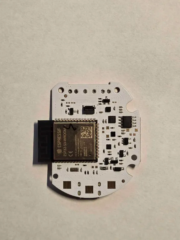

ESP32 Module (By both me (N4A) and princesspi3)
This is a reference pic of how the one on the FCC Filings look like (FCC Internal Photos for SWALLOWUNI)

Made/shared by princesspi3 (From a real Unit)

And i have a bare diagram for UART on the ESP-32 Itself (3V3/3.3v, GND, TX00, RX00) (I didnt wire BOOT cuz i lwk forgot, but the idea i guess is there.)
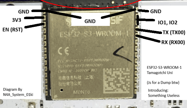
UART Diagram (The real Deal!, but it's disabled :c )

Quick crospin reference pic (For anyone who wants to check where the pins go for Power or smth idk) (DO NOT USE AS REFENCE FOR UART, JS FOR WHERE 3.3V LIVE ON THE PCB)

Now onto our third topic of the moment:
UART and JTAG
These are on a interesting situation i must admit, since while the UART Pins are exposed (And have been wired), but due to the OTP and eFuses are on the ESP32
Which means out only way to get a Unencrypted SPI Flash DUMP IS:
ALSO DISCLAMER: I DON'T (N4A) OWN ANY Tamagotchi Uni DEVICE. NOR BE RESPONSABLE OF THE DAMAGE/GORE OR CONSEUQUENCES OF THE RESOULTS TOWARDS YOUR UNIT/UNITS.
Now to start...
What do we know about the Uni? (Information derived from this thread, FCC Aplication 1 (.gov), FCC Aplication 2 (fccid.io), Some notes by princesspi3 and a few photos from cirip (Discord, Thanks a lot btw!))
- Its ESP32-S3 Based. (ESP32-S3-WROOM-1-N16) (Chip reference page here, Errata page here) And for those wondering its a S3R8. (Due to the 8 MB of PSRAM)
- Xtensa dual-core 32-bit LX7 microprocessor, up to 240MHz
- (I guess the clock is generated by the chip, but i know it supports an external clock signal, although i cant quite comprehend the use for it)
- Has a 16 MB (128 Mbit) Quad SPI Flash
- Uniform Block sectors of either 4/32/64 K-Byte.
- 128-bit Unique ID for each device.
- Serial Flash Discoverable parameters (SFDP) register
- It also has "Software/Hardware Write Protection"
- "Write protect all/portion of memory via software"
- "Enable/Disable protection with WP# Pin"
- "Top/Bottom Block protection"
- And sadly, OTP Protection. "3x1024-Byte Security Registers With OTP Locks"
- But for the rest of things, its a run of the mill / normal Quad SPI Flash
- 384 KB of ROM (programmed at factory) (On the ESP-32 Chipset?) (See table and page 392 of Technical manual, some memory addresses map multiple to the same location/data)
- ROM-0: 256 KB Area
- ROM-1: 128 KB Area
- 8MB Octal PSRAM (SPI Octal)
- 512 KB SRAM (A 16 KB or the total 32 KB of SRAM-0 memory space can be configured as instruction cache (ICache) to store instructions or read-only data of the external memory. In this case, the occupied memory space cannot be accessed by the CPU, while the remaining can still can be accessed by the CPU.)
- 16 KB SRAM in RTC
- I/O
- 3x UART Ports! (Factory flashing could have used one... and i have wired it out...)
- 2x I2C (Screen Interface and accelerometer maybe?)
- 1x USB Serial / JTAG Controller
- 1 x SDIO Host Controller with 2 slots.
- A General DMA Controller (GDNA) with 5 transmit channels and 5 receive channels.
- Has two Low Power CPUs:
- ULP-RISC-V coprocessor.
- ULP-FSM coprocessor.
- Security Features
- UART is diasabled!
- Secure Boot
- Flash Encryption
- 4-Kbit OTP (Up to 1792 bits for users, which means 2,304 bits are strictly reserved, and the leftovers could have been used by Bandai for locking UART or high-security control switches, cryptographic keys, and device identity flags that dictate how the bootloader and system recovery operate.... But i guess Bandai wouldn't go so far, and once again i remind you this is pure especulation, so maybe they did or maybe they didnt. Better safe than sorry.)
- A Hardware accelerated cryptographic engine for:
- AES-128 and 256 (FIPS PUB 197)
- Hashing (FIPS PUB 180-4)
- RSA
- RNG (Random Number Generator)
- HMAC
- Or Digital Signing.
- Xtensa dual-core 32-bit LX7 microprocessor, up to 240MHz
And for the device itself now,
We know the PCB: (Courtesy of cirip on Discord)
ESP32 Module (By both me (N4A) and princesspi3)
This is a reference pic of how the one on the FCC Filings look like (FCC Internal Photos for SWALLOWUNI)
Made/shared by princesspi3 (From a real Unit)
And i have a bare diagram for UART on the ESP-32 Itself (3V3/3.3v, GND, TX00, RX00) (I didnt wire BOOT cuz i lwk forgot, but the idea i guess is there.)
UART Diagram (The real Deal!, but it's disabled :c )
Quick crospin reference pic (For anyone who wants to check where the pins go for Power or smth idk) (DO NOT USE AS REFENCE FOR UART, JS FOR WHERE 3.3V LIVE ON THE PCB)
Now onto our third topic of the moment:
UART and JTAG
These are on a interesting situation i must admit, since while the UART Pins are exposed (And have been wired), but due to the OTP and eFuses are on the ESP32
- 4-Kbit OTP (Up to 1792 bits for users, which means 2,304 bits are strictly reserved, and the leftovers could have been used by Bandai for locking UART or high-security control switches, cryptographic keys, and device identity flags)
- UART
- JTAG
- USB Debugging
Which means out only way to get a Unencrypted SPI Flash DUMP IS:
- Desolder and/or Read the raw SPI data off the Uni (which has been done sucessfully, we js need a Sacrifice Uni Unit!)
- Somehow get the eFuse and ROM settings and data off the ESP32 (princesspi3 has been working on a voltage glitching teqnique)
- Decrypt the SPI
- And then...
- Profit! (Or well, see the SPI data... And finally figure out everything of the Device!!!)


