



Preface:
This is an essay, of sorts, compiling all of the information about the DSI Capture Card that I could find. Information may be missing or inaccurate, but what I present is my current understanding of the project.
I’ll start with the story and go into as much of the technical side as I can manage. If you wish to skip the story, head to the “Hardware” and "Software" sections.
If I come across any information that may be useful, I'll be sure to make an edit on this post.
Is there a practical reason to have a DSi capture card when the Original DS and the New 3DS/2DS family of systems can do everything the DSi can do and more?
No, no, there isn’t.
For someone like me who adores the DSi platform, the idea and novelty of a DSi capture card is very interesting to me. From the inception of the DSi Nistro Capture System to the soon-to-be-released DSi/DSi XL capture board by Merki, I have to give special thanks to the Internet Archive’s Wayback Machine for archiving these various webpages.
Katsukity was the sole provider of DSi Capture systems and a major player in the DS/3DS capture system provider and installer market in the mid to late 2010s.

Sometime between September 8th and 13th of 2016, the DSI Capture systems were removed from Katsukity’s shop. The dates are based on the Wayback Machine's captures of Katsukity's store website, so the exact timing is unknown.
I could not find a direct reason for why Katsukity halted the sales of the DSi Capture System. No blog entry, Twitter (X) post, or forum post spoke of it from what I was able to find/access.
On the storefront item ranking for sold items, the DSi capture systems never broke into the top ten, remaining at #11 and below. Once the New 3DS series of consoles was released, and a capture card was developed for it, the New 3DS systems quickly became the dominant system. The DSi Capture Systems disappeared from those charts, never to break into it for the remainder of the website's life (or at least as far as The Wayback Machine's images are concerned).
I mean, when you're spending up to and over $400 on a capture system, you are going to get the best one on the market: the New 3DS.
A quote from the Nisetoro Wiki suggested the installation was difficult, as over 40 cables were needed. On the store page, you can see how a custom bottom shell was needed to house that capture unit. I can infer that a combination of minimal interest and difficulty of installation is what led to the DSi Capture system being removed from the store.
On February 2nd, 2019, Twitter (X) user u/Really_Tall reposted a u/akiba365 tweet from February 1st claiming that Katsukity's business, Keity Co, Ltd., went bankrupt.

Their main Twitter (X) profile has been inactive since July 2018, their YouTube has been inactive since June 2018, and their digital storefront and blog have all been shuttered ( I won't hyperlink these two as one redirects to a scam. See archived links if you want to see them). Their Facebook Page also seems to have suffered the same fate, but I cannot confirm that. From my current understanding, Katsukity has disappeared from the internet.
Katsukity’s partner in Europe, Stefan Merki, and American Inventor Neal Tew (Loopy) appear to still manufacture, install, and sell capture cards on their website. As of the writing of this post, Stefan is still active on the website’s Discord Page (see their website for the invite link), and Loopy is active on their forum.
It is on Merki’s Discord Server that I was able to find a lot of information regarding the DSi Capture System. The most important, being a video posted to NicoVideo by the user ピピン (Pippin/Pippin P.).
This video, dating back to May 21st, 2010, shows the process of making a Nisetoro Capture card for the DSi and its success (The videos loaded better for me on Firefox).


This is the second Nisetoro Capture System Pippin has made, with their first one being for the Original DS. Both Nisetoro Capture systems use the same FPGA Dev Board and Software (more on that later).


"Nisetoro" and "Nisetro" seem to be just different methods of translating the Japanese "偽トロ". It would seem that Pippin's file name "Nisetroi" is referencing the "i" in DSi.
I don't speak or read Japanese, nor is this super important to the content of this post, but this is just to clear up any confusion in the documentation and various websites.
Rummaging through Katsukity's websites, I found the listings for the DSi Capture System on their older Japanese storefront (before a domain change). And on the product page for the Blue DSi Capture System, it uses the same FPGA Dev board Pippin, with credit given to them and their blog.
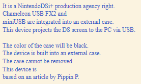
It all comes full circle.
Since Katsukity's closure, no modder or storefront has made or sold a DSi Capture System or Capture Card. The Dev board and software used for the capture card are woefully out of date and very difficult to obtain. In short, a capture board would have to be redone from scratch.
Which it has.
On July 18th, 2024, Loopy responded to their forum saying they are, in fact, working on a DSi, specifically the XL, capture board.

Nearly a year later, on June 14th, 2025, Stefan Merki announced on their Discord (invite link on Merki.net) that Capture Cards are on the way, with images of the prototype posted in their #general-discussion channel.

Instead of using the bulky Chameleon FX2, it would appear that Merki Loopy has made a custom board utilizing, from what I can make out, a Lattice ICE40 LP1K FPGA and FTDI USB controller. It appears to be a similar setup to their New 3DS capture system boards.
Prototype
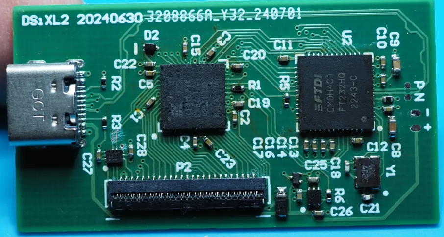
Final Revision

(When more information about the Merki capture console is available, I'll be sure to add it.)
The folks over on Merki.net aim to not just revive the concept of a DSi capture card, but modernize and add it seamlessly into the stock DSi and DSi XL shells. And though it is not ready for the retail market, I eagerly await the day I can purchase and install one for myself.
Take the following sections as historical information on the Nisetro Capture Systems.
Katsukity’s English store page for the DSI capture kits mentions a "Cameron USB FX2". I could not find anything on this capture device. This differs from the development board Pippin P used, a Chameleon USB FX2.
In Japan, where Katsuity is located, gamecapture.jp was their main Japanese storefront. Images of that site do not go back far enough to include the DSi capture systems, but that seems to be due to the site changing domains. The precursor website, cart05.lolipop.jp, dates back far enough to include the DSi capture systems. The capture card mentioned was indeed a Chameleon board.
Credit was given to Pippin on the 2011 capture of the Blue DSi Capture System page, but was not credited in the Dec 27th, 2011, and Jan 12th, 2014 item pages for the White Capture System. Specifically, for the 2014 page, credit is given to "an article posted on the blog." As of the writing of this, I have not found that blog, nor do I know the reason why credit to Pippin was withdrawn. Pippin's Blog was still around up until April 18th, 2016, when it was shut down, so you cannot claim it was because the blog shut down.
Reddit and GBA Temp user Lime_Cupboard purchased a suspected Katsukity capture unit. They provided some images of their capture unit.
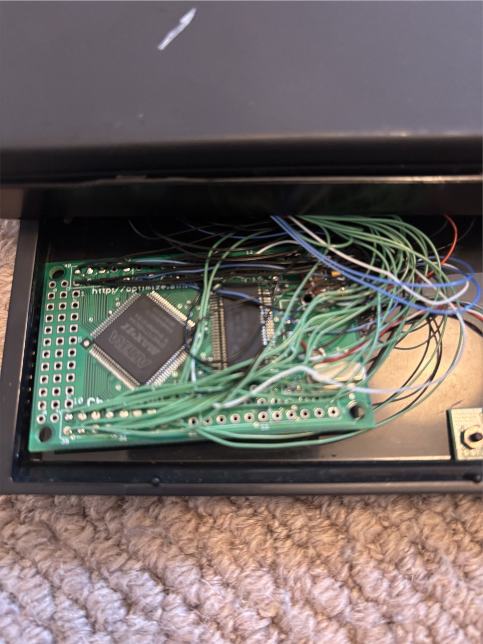
I also got my hands on a capture system, and the innards look the same.


The project boards match up with the one stated on the Japanese storefront page; the same board Pippin used.
In Pippin’s video, all of the test pins tapped and attached to a Chameleon FX2 USB were listed on their blog.

There, with the pinout sheet in a ZIP file containing various pieces of software (more on that later). I translated the parts into English.

On the NisetroInside website/blog, the process for creating a capture card for the Original DS was explained further. I can only vaguely see the images of the Chameleon board that Pippin has in their blog, but as far as I can tell, it is the same board. Pippin P's blog is also mentioned by name, so there is enough credit there.
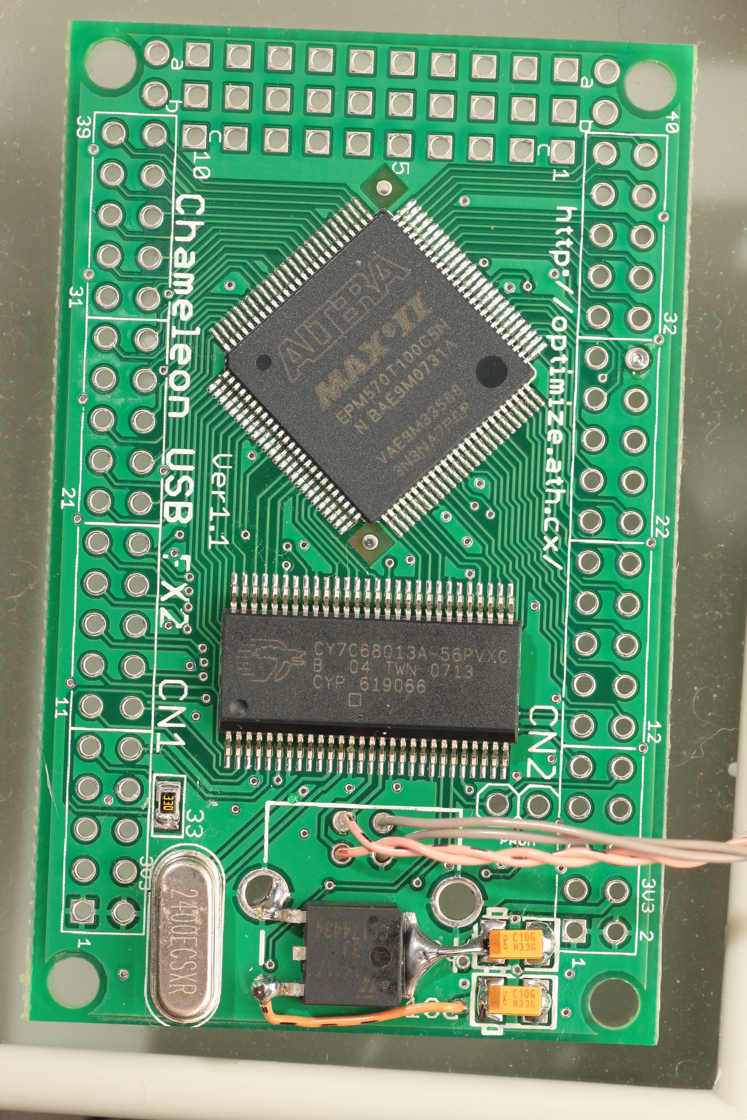
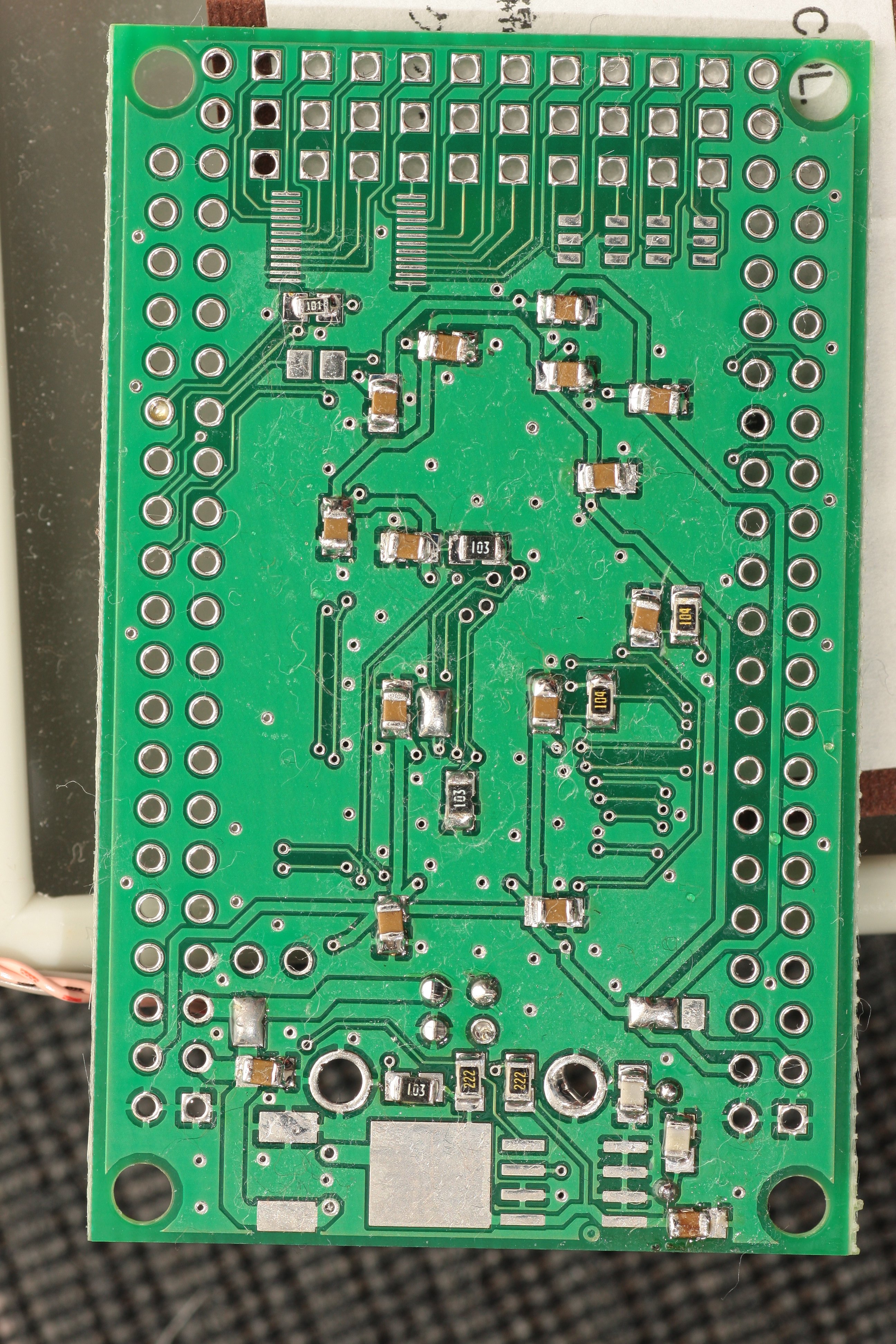
Following the link on the board to this website with the Chameleon USB FX2 featured prominently as a “Hot” item. When searching their shop, which is local only as far as I can tell, the Chameleon USB FX2 MiniB Kit is out of stock and appears to have been discontinued in 2019 (If it means anything, that board version was V1.2 instead of V1.1, so even if it was available, I do not know if that’d cause issues). I contacted the board seller, but they were unwilling to offer kits (it's within their right, but a bit frustrating).

Assembly instructions and software for the kit were available on their website along with the list of components, the Gerber file, and the Wire Schematic file. The Gerber file was, as far as I could tell, useless as it only shows one layer (The silkscreen, I think). That may be a consequence of modern Gerber viewers trying to read the file, or intentional, to keep people from printing their own boards. I tried multiple Gerber viewers, and the output was the same.
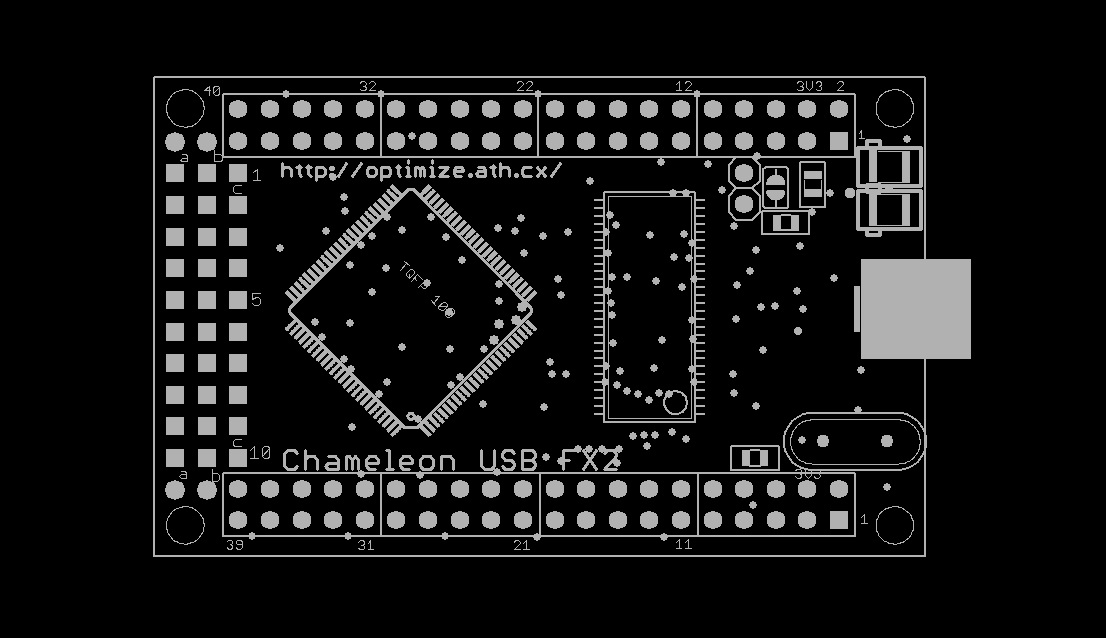
Searching Google for the Chameleon brings up an OSHPark shared file of a Chameleon USB FX2 by user splash5. Though this board appears to use the same chips, its circuit layout and components look entirely different than the one Pippin used and the one on the “How to make a Fake tro capture” page. To my untrained eyes, the traces go to different places which leads me to believe this board would never work.
Going through splash5’s Github page, it would seem they are implementing a Chameleon for game capture on the WonderSwan.
That is the first major hurdle. Where can I get a comparable board? Does the Chameleon USB FX2 need to be recreated from the images in these forums?
Their blog, which can only be accessed through Internet Archive’s Wayback Machine, has their project as well as a ZIP containing the pinout for the DSI to Chameleon USB connection and various files (.svf, .dpf, .pin, .pof, .qpf,.qsf and .v)

Opening the various files in Notepad++ reveals that Pippin used the Quartus II Design Environment from Intel/Altera for this project. The Quartus II Version 9.1 software used is no longer available to download through Intel, and though it is common practice to be wary of random executable files, an archived version of the software is on Archive.org as of the writing of this post. It may no longer be useful in today's atmosphere, but it is what was used to create this project.
I'll try to have the most important code here for posterity, but I'm hitting character limits. A paste of each file's content will be available on Pastebin except the .svf file, as it is too long.
Going through each file:
A Readme file (In Japanese)
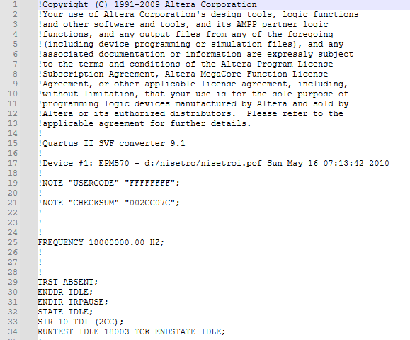
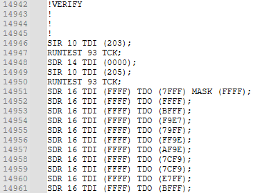
An ASCII text file (with the extension .svf) that stores programming data for programming, verifying, and blank-checking one or more fixed-algorithm devices in a JTAG chain in Automated Test Equipment (ATE)-type programming environments.
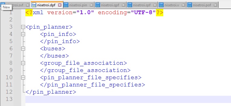
The Design Protocol File (.dpf) is a software information storage for the Quartus environment.
The Pin Assignment File (.pin) contains the I/O pin name, number location, direction, and I/O standard for all used and unused pins within the design.
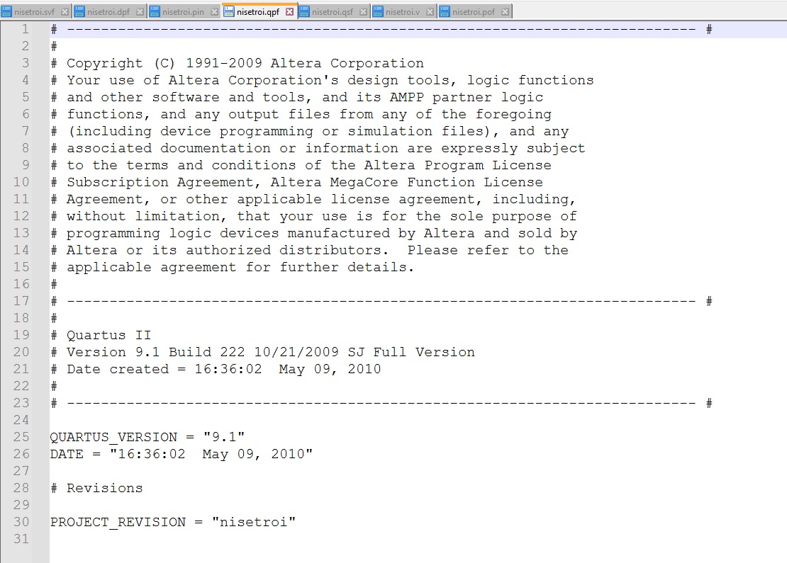
The Quartus Prime Project File (.qpf) contains basic information about the version of Quartus used. It also lists the revisions for the project. In this case, the name of the project.
The Quartus Prime Setting File (.qsf) contains project and entry-level assignments and settings for the project.
The Verilog Design Fil (.v) for the project.
Lastly, the Programmer Object File (.pof) which contains the data for programming the MAX II (one main chip on the Chameleon board). When opening the file in the Quartus II version 9.1 software, it appears it wants to upload to something, presumably, the MAX II. I assume this is the compiled file ready to upload to the MAX II.

If you are uncertain of the condition of your capture system, my advice is to try the capture software on another computer if you're experiencing issues.
A backup on NiseTroPreview20100316 is available on Github in case the archive goes offline.
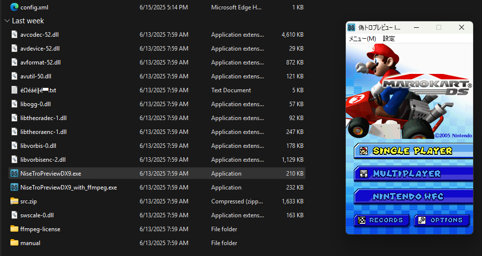
On my capture system, Win 11 didn't automatically recognize the device, labeling it as "unknown". Drivers for the FX2 are still provided through Infineon. Download the "EZ-USB™ FX2LP CY3684 Development kit setup", install, and update the drivers with the file path pointing to the Cypress folder on your C drive (this is done in the device manager). (The drivers with the next program, cc3dsfs, also seem to work with this program as well.)
The software is in Japanese without an option to switch to English. If you want to continue using this program, I would either familiarize yourself with the options and where they are, or use a tool like Resource Hacker to change the text within the .exe. I did that, and it worked great.

Other than that, it is a bare-bones capture software. The settings in the image above are the only meaningful options. This is in stark contrast to the next program: cc3dsfs.
I compiled and used the program on my personal capture card, and it works great.
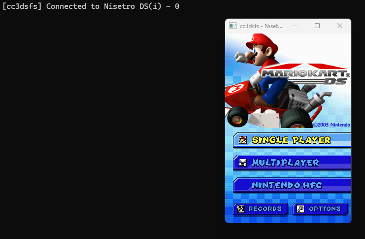
I haven't had a good chance to explore the options with the sheer amount there are. Being able to split the screens into their own windows is very nice.
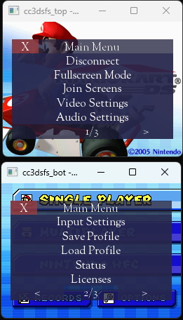
CC3DSFS didn't have an updated official release of the software, but an automatic nightly build of the .exe is available.
The viewing software is locked behind a product key that ships with your device. From what I understand, it has to match your system ID, so no random product key will work.
Non-Standard only hosts software for the 3DS platform. I was unable to find a DS variant of the software, if it exists, but it stands to reason that they bundle the DS viewer into the 3DS viewing software.
One archived version of the DS_View software exists on Archive.org that I was able to find, but, same problem, it is locked behind a product key.
I have this pie-in-the-sky dream of assembling and using a DSi XL with a capture card in it, but what my research dug up was a need for commissioning people much smarter than I to create the capture board and injecting the code.
That is simply something I can not do right now.
The Chameleon kits are simply impossible to find, or have just been left behind for better project boards.
If I wanted to get my hands on a Chameleon board, I'd either have to get the PCB print file from the creator/license holder or somehow recreate it myself. I can tell you right now that is beyond my current abilities.
I am, however, somewhat confident that the software that is loaded onto the Chameleon and Capture program still exists, leaving the challenge of a DSi Capture device solely on the board kit. (Merki.net is developing a DSi and DSi XL capture system).
For anyone who reads this, I do hope that this pinout I made is helpful.

This is a pinout referencing the pinout from Pippin as well as the DSi XL test points on DSiBrew. I have to trust it is accurate, as I do not know of a way to test it otherwise. Entries highlighted in Red have the same comment, but the numbering sequence suggests the order I put them is correct.
Anyway, that is enough for me.
I originally posted this on Reddit, but I was very interested in hearing what everyone here has to say.
This is an essay, of sorts, compiling all of the information about the DSI Capture Card that I could find. Information may be missing or inaccurate, but what I present is my current understanding of the project.
I’ll start with the story and go into as much of the technical side as I can manage. If you wish to skip the story, head to the “Hardware” and "Software" sections.
If I come across any information that may be useful, I'll be sure to make an edit on this post.
=====Story====
Introduction:
Is there a practical reason to have a DSi capture card when the Original DS and the New 3DS/2DS family of systems can do everything the DSi can do and more?
No, no, there isn’t.
For someone like me who adores the DSi platform, the idea and novelty of a DSi capture card is very interesting to me. From the inception of the DSi Nistro Capture System to the soon-to-be-released DSi/DSi XL capture board by Merki, I have to give special thanks to the Internet Archive’s Wayback Machine for archiving these various webpages.
Body:
Katsukity was the sole provider of DSi Capture systems and a major player in the DS/3DS capture system provider and installer market in the mid to late 2010s.
Sometime between September 8th and 13th of 2016, the DSI Capture systems were removed from Katsukity’s shop. The dates are based on the Wayback Machine's captures of Katsukity's store website, so the exact timing is unknown.
I could not find a direct reason for why Katsukity halted the sales of the DSi Capture System. No blog entry, Twitter (X) post, or forum post spoke of it from what I was able to find/access.
On the storefront item ranking for sold items, the DSi capture systems never broke into the top ten, remaining at #11 and below. Once the New 3DS series of consoles was released, and a capture card was developed for it, the New 3DS systems quickly became the dominant system. The DSi Capture Systems disappeared from those charts, never to break into it for the remainder of the website's life (or at least as far as The Wayback Machine's images are concerned).
I mean, when you're spending up to and over $400 on a capture system, you are going to get the best one on the market: the New 3DS.
A quote from the Nisetoro Wiki suggested the installation was difficult, as over 40 cables were needed. On the store page, you can see how a custom bottom shell was needed to house that capture unit. I can infer that a combination of minimal interest and difficulty of installation is what led to the DSi Capture system being removed from the store.
On February 2nd, 2019, Twitter (X) user u/Really_Tall reposted a u/akiba365 tweet from February 1st claiming that Katsukity's business, Keity Co, Ltd., went bankrupt.
Their main Twitter (X) profile has been inactive since July 2018, their YouTube has been inactive since June 2018, and their digital storefront and blog have all been shuttered ( I won't hyperlink these two as one redirects to a scam. See archived links if you want to see them). Their Facebook Page also seems to have suffered the same fate, but I cannot confirm that. From my current understanding, Katsukity has disappeared from the internet.
Katsukity’s partner in Europe, Stefan Merki, and American Inventor Neal Tew (Loopy) appear to still manufacture, install, and sell capture cards on their website. As of the writing of this post, Stefan is still active on the website’s Discord Page (see their website for the invite link), and Loopy is active on their forum.
It is on Merki’s Discord Server that I was able to find a lot of information regarding the DSi Capture System. The most important, being a video posted to NicoVideo by the user ピピン (Pippin/Pippin P.).
This video, dating back to May 21st, 2010, shows the process of making a Nisetoro Capture card for the DSi and its success (The videos loaded better for me on Firefox).
This is the second Nisetoro Capture System Pippin has made, with their first one being for the Original DS. Both Nisetoro Capture systems use the same FPGA Dev Board and Software (more on that later).
>>> Quick Aside >>>
As for the name of the project, Nisetoro/Nisetro Capture (Fake Toro/ Fake Tro Capture), Pippin and Katsukity describe it as a pun "(false (nise, fake) + nitro (nitoro, nitro) = nisetro)". Nitro is the code name for the Original DS console as well as a reference to the IS-NITRO development and capture kits. The discrepancy between"Nisetoro" and "Nisetro" seem to be just different methods of translating the Japanese "偽トロ". It would seem that Pippin's file name "Nisetroi" is referencing the "i" in DSi.
I don't speak or read Japanese, nor is this super important to the content of this post, but this is just to clear up any confusion in the documentation and various websites.
>>>>>>>>>>>>>>>>>
And just like Katsukity, Pippin P seems to have also disappeared from the internet. Their Blog was shuttered, and their NicoVideo account has been inactive since the posting of the DSi Nisetoro capture system. I know of no other blogs or social media that Pippin P. used or is actively using.Rummaging through Katsukity's websites, I found the listings for the DSi Capture System on their older Japanese storefront (before a domain change). And on the product page for the Blue DSi Capture System, it uses the same FPGA Dev board Pippin, with credit given to them and their blog.
It all comes full circle.
Since Katsukity's closure, no modder or storefront has made or sold a DSi Capture System or Capture Card. The Dev board and software used for the capture card are woefully out of date and very difficult to obtain. In short, a capture board would have to be redone from scratch.
Which it has.
On July 18th, 2024, Loopy responded to their forum saying they are, in fact, working on a DSi, specifically the XL, capture board.
Nearly a year later, on June 14th, 2025, Stefan Merki announced on their Discord (invite link on Merki.net) that Capture Cards are on the way, with images of the prototype posted in their #general-discussion channel.
Prototype
Final Revision
(When more information about the Merki capture console is available, I'll be sure to add it.)
Conclusion:
So, did the DSi Capture Card End with Katsukity? Well, when I first wrote this post back in May of 2024, yes, it did. Once Katsukity stopped selling capture units, no other outlet produced, spoke of, installed, or sold any type of capture card for the DSi. It was, effectively, left in the past, with the few surviving capture units rarely circulating on auction sites.The folks over on Merki.net aim to not just revive the concept of a DSi capture card, but modernize and add it seamlessly into the stock DSi and DSi XL shells. And though it is not ready for the retail market, I eagerly await the day I can purchase and install one for myself.
=================
All information below only concerns the Chameleon USB FX2 Capture Systems. I fully expect the capture card and code used to make Loopy/Merki's Capture System to be proprietary. They have a business to run, I understand that, but Katsukity's business took the information they had with them when their company went bankrupt.Take the following sections as historical information on the Nisetro Capture Systems.
====Hardware====
From here, I have to stick a disclaimer. As much as it pains me to say, anything involving Circuit Boards and programming is well beyond my understanding. I will provide any information I have regarding the components and software used for the project, but I will not pretend to understand any of it. Forgive my ignorance in advance.Katsukity’s English store page for the DSI capture kits mentions a "Cameron USB FX2". I could not find anything on this capture device. This differs from the development board Pippin P used, a Chameleon USB FX2.
In Japan, where Katsuity is located, gamecapture.jp was their main Japanese storefront. Images of that site do not go back far enough to include the DSi capture systems, but that seems to be due to the site changing domains. The precursor website, cart05.lolipop.jp, dates back far enough to include the DSi capture systems. The capture card mentioned was indeed a Chameleon board.
Credit was given to Pippin on the 2011 capture of the Blue DSi Capture System page, but was not credited in the Dec 27th, 2011, and Jan 12th, 2014 item pages for the White Capture System. Specifically, for the 2014 page, credit is given to "an article posted on the blog." As of the writing of this, I have not found that blog, nor do I know the reason why credit to Pippin was withdrawn. Pippin's Blog was still around up until April 18th, 2016, when it was shut down, so you cannot claim it was because the blog shut down.
Reddit and GBA Temp user Lime_Cupboard purchased a suspected Katsukity capture unit. They provided some images of their capture unit.
I also got my hands on a capture system, and the innards look the same.
>>> Quick Aside >>>
The housing for the capture card looks to be a modified Playtech Multifunction Crystal Case w/ Storage Tray. I haven't been able to find an unboxed product image, but the cutouts for the shoulder buttons and tray look identical.>>>>>>>>>>>>>>>>>
The project boards match up with the one stated on the Japanese storefront page; the same board Pippin used.
In Pippin’s video, all of the test pins tapped and attached to a Chameleon FX2 USB were listed on their blog.
There, with the pinout sheet in a ZIP file containing various pieces of software (more on that later). I translated the parts into English.
On the NisetroInside website/blog, the process for creating a capture card for the Original DS was explained further. I can only vaguely see the images of the Chameleon board that Pippin has in their blog, but as far as I can tell, it is the same board. Pippin P's blog is also mentioned by name, so there is enough credit there.
Following the link on the board to this website with the Chameleon USB FX2 featured prominently as a “Hot” item. When searching their shop, which is local only as far as I can tell, the Chameleon USB FX2 MiniB Kit is out of stock and appears to have been discontinued in 2019 (If it means anything, that board version was V1.2 instead of V1.1, so even if it was available, I do not know if that’d cause issues). I contacted the board seller, but they were unwilling to offer kits (it's within their right, but a bit frustrating).
Assembly instructions and software for the kit were available on their website along with the list of components, the Gerber file, and the Wire Schematic file. The Gerber file was, as far as I could tell, useless as it only shows one layer (The silkscreen, I think). That may be a consequence of modern Gerber viewers trying to read the file, or intentional, to keep people from printing their own boards. I tried multiple Gerber viewers, and the output was the same.
Searching Google for the Chameleon brings up an OSHPark shared file of a Chameleon USB FX2 by user splash5. Though this board appears to use the same chips, its circuit layout and components look entirely different than the one Pippin used and the one on the “How to make a Fake tro capture” page. To my untrained eyes, the traces go to different places which leads me to believe this board would never work.
Going through splash5’s Github page, it would seem they are implementing a Chameleon for game capture on the WonderSwan.
That is the first major hurdle. Where can I get a comparable board? Does the Chameleon USB FX2 need to be recreated from the images in these forums?
The Chameleon USB FX2 uses two main ICs:
- The Cypress High-Speed USB Peripheral Controller CY7C68013A-56PVXC
- The Altera Max II Complex Programmable Logic Device (CPLD) EPM570T100C5N
The description of the Chameleon from Optimize's website:
The Chameleon USB FX2 can be used as a high-speed, high-capacity data logger/generator on its own.
This application was developed in a laboratory of a national university to acquire and analyze GPS data. All the source code is open to the public, so I think it can be used for various purposes by improving it.
- The Cypress High-Speed USB Peripheral Controller CY7C68013A-56PVXC
- The Altera Max II Complex Programmable Logic Device (CPLD) EPM570T100C5N
The description of the Chameleon from Optimize's website:
The Chameleon USB FX2 can be used as a high-speed, high-capacity data logger/generator on its own.
This application was developed in a laboratory of a national university to acquire and analyze GPS data. All the source code is open to the public, so I think it can be used for various purposes by improving it.
- Data can be stored on the PC's HDD via USB, allowing virtually unlimited data to be recorded
- Logged data can be output externally using generator software (external clock input required)
- The recording speed is affected by the HDD write speed of the PC, but 20MHz on a normal desktop HDD OK UP TO ABOUT 16CH
- Selectable 2/4/8/16 channels with a maximum sampling clock of 100 MHz
- It can detect when the USB transfer speed cannot keep up and data is dropped, so continuous data can be acquired.
- Data sampling is clock rise, data output is clock rise and fall
- FX2's 48MHz divided 24/12/6/3/1.5Mz clock is output from the I/O pins
- Cypress EZ-USB FX2LP(CY7C68013A-56) EPM570T100 +
- The FX2LP FIFO and MAX2 are directly connected inside the board, enabling data transfer between the PC and MAX2 at speeds exceeding 300Mbps.
- Since it is a USB connection, it can be used with a notebook PC and can be used anywhere, and there is no need for a separate power supply.
- The MAX2 can be written via USB. (No need for dedicated writing hardware)
- The EZ-USB firmware can be downloaded as required by individual applications on the PC side. It can be used for various purposes simply by rewriting the MAX2 and changing the connection destination. (This is where the chameleon comes from.)
- Development tools (FX2LP, MAX2) are available free of charge.
- MAX2 57 IOs and 570 logic elements are freely available.
The 48MHz clock provided by the FX2LP can be used with MAX2 logic. - The MAX2 supports a variety of standard I/O standards (3.3V/2.5V/1.8V/1.5V) and provides flexible power management such as hot-swapping and hot-socketing.
- Since there is a universal area in the PCB, it is possible to assemble a simple circuit on the board.
- TTL for voltage level translation can be implemented in a universal area, allowing interfacing with 5V I/O.
- Standard firmware and simple, easy-to-use libraries are provided in the source code, making application development more efficient for users.
- Ideal for learning USB, VHDL, and Verilog.
- The EZ-USB FX2 is equipped with a programmable interface called GPIF, so it can be easily connected to a parallel bus or an IDE bus on a hard disk. However, recent buses have been changed from parallel buses to serial buses. (Hard disks are also migrating from IDE (parallel) to SATA (serial). The FX2LP cannot support serial data by itself.
- In addition, cameras and TV broadcasts are switching from analog to digital, and communication speeds are also increasing.
- Under these circumstances, in order to easily handle high-speed digital data in special-purpose equipment, hobby and R&D, "Chameleon USB FX2".
- Collecting data with the FX2LP and MAX2 (CPLD) and performing digital processing on the high-performance CPU of a PC will open up various possibilities.
====Toolchain Software====
For the software side, it is my understanding that Pippin already provided it within the ZIP. In the description of their video, they say that the software is the same as the Original DS. This is, of course, assuming that the software is the same as the one used back in 2010.Their blog, which can only be accessed through Internet Archive’s Wayback Machine, has their project as well as a ZIP containing the pinout for the DSI to Chameleon USB connection and various files (.svf, .dpf, .pin, .pof, .qpf,.qsf and .v)
Opening the various files in Notepad++ reveals that Pippin used the Quartus II Design Environment from Intel/Altera for this project. The Quartus II Version 9.1 software used is no longer available to download through Intel, and though it is common practice to be wary of random executable files, an archived version of the software is on Archive.org as of the writing of this post. It may no longer be useful in today's atmosphere, but it is what was used to create this project.
I'll try to have the most important code here for posterity, but I'm hitting character limits. A paste of each file's content will be available on Pastebin except the .svf file, as it is too long.
Going through each file:
A Readme file (In Japanese)
適当に作ってみるといいよ。
システム的にキャプチャ部分(クロック・下画面・上画面)とオーディオ部分は連動していないので、
オーディオがいらない場合はキャプチャ部分の配線だけでOK。
逆にデジタルオーディオだけが欲しい場合はオーディオだけの配線でOK(それなら専用IC使うほうがいいが・・・)
オーディオ出力は32kHz16bitなので大抵のアンプ・スピーカーで受信できると思います。
キャプチャ部分は偽トロキャプチャと互換です。
注意
DSiはDSに比べて内部の余剰スペースが非常に少ないのでDSiを元のケースに戻したい場合、
0.2mmのUEW等、外径が細い線を使う必要があります。
SPDIFに使用するTOSLINKは3.3vの物ならそのまま使用できます。
5vのTOSLINKはレベルコンバータが必要かもしれません。
システム的にキャプチャ部分(クロック・下画面・上画面)とオーディオ部分は連動していないので、
オーディオがいらない場合はキャプチャ部分の配線だけでOK。
逆にデジタルオーディオだけが欲しい場合はオーディオだけの配線でOK(それなら専用IC使うほうがいいが・・・)
オーディオ出力は32kHz16bitなので大抵のアンプ・スピーカーで受信できると思います。
キャプチャ部分は偽トロキャプチャと互換です。
注意
DSiはDSに比べて内部の余剰スペースが非常に少ないのでDSiを元のケースに戻したい場合、
0.2mmのUEW等、外径が細い線を使う必要があります。
SPDIFに使用するTOSLINKは3.3vの物ならそのまま使用できます。
5vのTOSLINKはレベルコンバータが必要かもしれません。
An ASCII text file (with the extension .svf) that stores programming data for programming, verifying, and blank-checking one or more fixed-algorithm devices in a JTAG chain in Automated Test Equipment (ATE)-type programming environments.
The Design Protocol File (.dpf) is a software information storage for the Quartus environment.
The Pin Assignment File (.pin) contains the I/O pin name, number location, direction, and I/O standard for all used and unused pins within the design.
Code:
-- Copyright (C) 1991-2009 Altera Corporation
-- Your use of Altera Corporation's design tools, logic functions
-- and other software and tools, and its AMPP partner logic
-- functions, and any output files from any of the foregoing
-- (including device programming or simulation files), and any
-- associated documentation or information are expressly subject
-- to the terms and conditions of the Altera Program License
-- Subscription Agreement, Altera MegaCore Function License
-- Agreement, or other applicable license agreement, including,
-- without limitation, that your use is for the sole purpose of
-- programming logic devices manufactured by Altera and sold by
-- Altera or its authorized distributors. Please refer to the
-- applicable agreement for further details.
--
-- This is a Quartus II output file. It is for reporting purposes only, and is
-- not intended for use as a Quartus II input file. This file cannot be used
-- to make Quartus II pin assignments - for instructions on how to make pin
-- assignments, please see Quartus II help.
---------------------------------------------------------------------------------
---------------------------------------------------------------------------------
-- NC : No Connect. This pin has no internal connection to the device.
-- DNU : Do Not Use. This pin MUST NOT be connected.
-- VCCINT : Dedicated power pin, which MUST be connected to VCC (2.5V/3.3V).
-- VCCIO : Dedicated power pin, which MUST be connected to VCC
-- of its bank.
-- Bank 1: 3.3V
-- Bank 2: 3.3V
-- GND : Dedicated ground pin. Dedicated GND pins MUST be connected to GND.
-- It can also be used to report unused dedicated pins. The connection
-- on the board for unused dedicated pins depends on whether this will
-- be used in a future design. One example is device migration. When
-- using device migration, refer to the device pin-tables. If it is a
-- GND pin in the pin table or if it will not be used in a future design
-- for another purpose the it MUST be connected to GND. If it is an unused
-- dedicated pin, then it can be connected to a valid signal on the board
-- (low, high, or toggling) if that signal is required for a different
-- revision of the design.
-- GND+ : Unused input pin. It can also be used to report unused dual-purpose pins.
-- This pin should be connected to GND. It may also be connected to a
-- valid signal on the board (low, high, or toggling) if that signal
-- is required for a different revision of the design.
-- GND* : Unused I/O pin. For transceiver I/O banks (Bank 13, 14, 15, 16 and 17),
-- connect each pin marked GND* either individually through a 10k Ohm resistor
-- to GND or tie all pins together and connect through a single 10k Ohm resistor
-- to GND.
-- For non-transceiver I/O banks, connect each pin marked GND* directly to GND
-- or leave it unconnected.
-- RESERVED : Unused I/O pin, which MUST be left unconnected.
-- RESERVED_INPUT : Pin is tri-stated and should be connected to the board.
-- RESERVED_INPUT_WITH_WEAK_PULLUP : Pin is tri-stated with internal weak pull-up resistor.
-- RESERVED_INPUT_WITH_BUS_HOLD : Pin is tri-stated with bus-hold circuitry.
-- RESERVED_OUTPUT_DRIVEN_HIGH : Pin is output driven high.
---------------------------------------------------------------------------------
---------------------------------------------------------------------------------
-- Pin directions (input, output or bidir) are based on device operating in user mode.
---------------------------------------------------------------------------------
Quartus II Version 9.1 Build 222 10/21/2009 SJ Full Version
CHIP "nisetroi" ASSIGNED TO AN: EPM570T100C3
Pin Name/Usage : Location : Dir. : I/O Standard : Voltage : I/O Bank : User Assignment
-------------------------------------------------------------------------------------------------------------
GND* : 1 : : : : 2 :
GND* : 2 : : : : 1 :
MODE[0] : 3 : input : 3.3-V LVTTL : : 1 : Y
MODE[1] : 4 : input : 3.3-V LVTTL : : 1 : Y
FX2_SLRD : 5 : output : 3.3-V LVTTL : : 1 : Y
FX2_SLWR : 6 : output : 3.3-V LVTTL : : 1 : Y
RESET : 7 : input : 3.3-V LVTTL : : 1 : Y
DIR : 8 : input : 3.3-V LVTTL : : 1 : Y
VCCIO1 : 9 : power : : 3.3V : 1 :
GNDIO : 10 : gnd : : : :
GNDINT : 11 : gnd : : : :
GND* : 12 : : : : 1 :
VCCINT : 13 : power : : 2.5V/3.3V : :
FX2_IFCLK : 14 : input : 3.3-V LVTTL : : 1 : Y
ADDR[2] : 15 : input : 3.3-V LVTTL : : 1 : Y
ADDR[1] : 16 : input : 3.3-V LVTTL : : 1 : Y
ADDR[0] : 17 : input : 3.3-V LVTTL : : 1 : Y
FX2_PKTEND : 18 : output : 3.3-V LVTTL : : 1 : Y
FX2_FIFOADR[1] : 19 : output : 3.3-V LVTTL : : 1 : Y
FX2_FIFOADR[0] : 20 : output : 3.3-V LVTTL : : 1 : Y
FX2_SLOE : 21 : output : 3.3-V LVTTL : : 1 : Y
TMS : 22 : input : : : 1 :
TDI : 23 : input : : : 1 :
TCK : 24 : input : : : 1 :
TDO : 25 : output : : : 1 :
FX2_FLAGC : 26 : input : 3.3-V LVTTL : : 1 : Y
FX2_FLAGB : 27 : input : 3.3-V LVTTL : : 1 : Y
FX2_FLAGA : 28 : input : 3.3-V LVTTL : : 1 : Y
FX2_FD[7] : 29 : bidir : 3.3-V LVTTL : : 1 : Y
FX2_FD[6] : 30 : bidir : 3.3-V LVTTL : : 1 : Y
VCCIO1 : 31 : power : : 3.3V : 1 :
GNDIO : 32 : gnd : : : :
FX2_FD[5] : 33 : bidir : 3.3-V LVTTL : : 1 : Y
FX2_FD[4] : 34 : bidir : 3.3-V LVTTL : : 1 : Y
FX2_FD[0] : 35 : bidir : 3.3-V LVTTL : : 1 : Y
FX2_FD[1] : 36 : bidir : 3.3-V LVTTL : : 1 : Y
GNDINT : 37 : gnd : : : :
FX2_FD[2] : 38 : bidir : 3.3-V LVTTL : : 1 : Y
VCCINT : 39 : power : : 2.5V/3.3V : :
FX2_FD[3] : 40 : bidir : 3.3-V LVTTL : : 1 : Y
SOUT : 41 : output : 3.3-V LVTTL : : 1 : Y
GND* : 42 : : : : 1 :
GND* : 43 : : : : 1 :
LCDB1[0] : 44 : input : 3.3-V LVTTL : : 1 : Y
VCCIO1 : 45 : power : : 3.3V : 1 :
GNDIO : 46 : gnd : : : :
LCDB1[1] : 47 : input : 3.3-V LVTTL : : 1 : Y
LCDB1[2] : 48 : input : 3.3-V LVTTL : : 1 : Y
LCDB1[3] : 49 : input : 3.3-V LVTTL : : 1 : Y
LCDB1[4] : 50 : input : 3.3-V LVTTL : : 1 : Y
LCDB1[5] : 51 : input : 3.3-V LVTTL : : 1 : Y
LCDR1[0] : 52 : input : 3.3-V LVTTL : : 2 : Y
LCDR1[1] : 53 : input : 3.3-V LVTTL : : 2 : Y
LCDR1[2] : 54 : input : 3.3-V LVTTL : : 2 : Y
LCDR1[3] : 55 : input : 3.3-V LVTTL : : 2 : Y
LCDR1[4] : 56 : input : 3.3-V LVTTL : : 2 : Y
LCDR1[5] : 57 : input : 3.3-V LVTTL : : 2 : Y
SND_WS : 58 : input : 3.3-V LVTTL : : 2 : Y
VCCIO2 : 59 : power : : 3.3V : 2 :
GNDIO : 60 : gnd : : : :
SND_SDO : 61 : input : 3.3-V LVTTL : : 2 : Y
CLK : 62 : input : 3.3V Schmitt Trigger Input : : 2 : Y
VCCINT : 63 : power : : 2.5V/3.3V : :
SND_MCLK : 64 : input : 3.3-V LVTTL : : 2 : Y
GNDINT : 65 : gnd : : : :
Hsync : 66 : input : 3.3V Schmitt Trigger Input : : 2 : Y
Vsync : 67 : input : 3.3V Schmitt Trigger Input : : 2 : Y
GND* : 68 : : : : 2 :
GND* : 69 : : : : 2 :
LCDG1[0] : 70 : input : 3.3-V LVTTL : : 2 : Y
LCDG1[1] : 71 : input : 3.3-V LVTTL : : 2 : Y
LCDG1[2] : 72 : input : 3.3-V LVTTL : : 2 : Y
LCDG1[3] : 73 : input : 3.3-V LVTTL : : 2 : Y
LCDG1[4] : 74 : input : 3.3-V LVTTL : : 2 : Y
LCDG1[5] : 75 : input : 3.3-V LVTTL : : 2 : Y
LCDG2[5] : 76 : input : 3.3-V LVTTL : : 2 : Y
LCDG2[4] : 77 : input : 3.3-V LVTTL : : 2 : Y
LCDG2[3] : 78 : input : 3.3-V LVTTL : : 2 : Y
GNDIO : 79 : gnd : : : :
VCCIO2 : 80 : power : : 3.3V : 2 :
LCDG2[2] : 81 : input : 3.3-V LVTTL : : 2 : Y
LCDG2[1] : 82 : input : 3.3-V LVTTL : : 2 : Y
LCDG2[0] : 83 : input : 3.3-V LVTTL : : 2 : Y
LCDR2[5] : 84 : input : 3.3-V LVTTL : : 2 : Y
LCDR2[4] : 85 : input : 3.3-V LVTTL : : 2 : Y
LCDR2[3] : 86 : input : 3.3-V LVTTL : : 2 : Y
LCDR2[2] : 87 : input : 3.3-V LVTTL : : 2 : Y
VCCINT : 88 : power : : 2.5V/3.3V : :
LCDR2[1] : 89 : input : 3.3-V LVTTL : : 2 : Y
GNDINT : 90 : gnd : : : :
LCDR2[0] : 91 : input : 3.3-V LVTTL : : 2 : Y
LCDB2[5] : 92 : input : 3.3-V LVTTL : : 2 : Y
GNDIO : 93 : gnd : : : :
VCCIO2 : 94 : power : : 3.3V : 2 :
LCDB2[4] : 95 : input : 3.3-V LVTTL : : 2 : Y
LCDB2[3] : 96 : input : 3.3-V LVTTL : : 2 : Y
LCDB2[2] : 97 : input : 3.3-V LVTTL : : 2 : Y
LCDB2[1] : 98 : input : 3.3-V LVTTL : : 2 : Y
LCDB2[0] : 99 : input : 3.3-V LVTTL : : 2 : Y
GND* : 100 : : : : 2 :The Quartus Prime Project File (.qpf) contains basic information about the version of Quartus used. It also lists the revisions for the project. In this case, the name of the project.
The Quartus Prime Setting File (.qsf) contains project and entry-level assignments and settings for the project.
Code:
# -------------------------------------------------------------------------- #
#
# Copyright (C) 1991-2009 Altera Corporation
# Your use of Altera Corporation's design tools, logic functions
# and other software and tools, and its AMPP partner logic
# functions, and any output files from any of the foregoing
# (including device programming or simulation files), and any
# associated documentation or information are expressly subject
# to the terms and conditions of the Altera Program License
# Subscription Agreement, Altera MegaCore Function License
# Agreement, or other applicable license agreement, including,
# without limitation, that your use is for the sole purpose of
# programming logic devices manufactured by Altera and sold by
# Altera or its authorized distributors.  Please refer to the
# applicable agreement for further details.
#
# -------------------------------------------------------------------------- #
#
# Quartus II
# Version 9.1 Build 222 10/21/2009 SJ Full Version
# Date created = 17:27:31  April 30, 2010
#
# -------------------------------------------------------------------------- #
#
# Notes:
#
# 1) The default values for assignments are stored in the file:
#        nisetroi_assignment_defaults.qdf
#    If this file doesn't exist, see file:
#        assignment_defaults.qdf
#
# 2) Altera recommends that you do not modify this file. This
#    file is updated automatically by the Quartus II software
#    and any changes you make may be lost or overwritten.
#
# -------------------------------------------------------------------------- #


set_global_assignment -name FAMILY "MAX II"
set_global_assignment -name DEVICE EPM570T100C3
set_global_assignment -name TOP_LEVEL_ENTITY nisetroi
set_global_assignment -name ORIGINAL_QUARTUS_VERSION 9.1
set_global_assignment -name PROJECT_CREATION_TIME_DATE "17:27:31  APRIL 30, 2010"
set_global_assignment -name LAST_QUARTUS_VERSION 9.1
set_global_assignment -name USE_GENERATED_PHYSICAL_CONSTRAINTS OFF -section_id eda_blast_fpga
set_global_assignment -name MIN_CORE_JUNCTION_TEMP 0
set_global_assignment -name MAX_CORE_JUNCTION_TEMP 85
set_global_assignment -name POWER_EXT_SUPPLY_VOLTAGE_TO_REGULATOR 3.3V
set_global_assignment -name VERILOG_FILE nisetroi.v
set_global_assignment -name MISC_FILE "d:/nisetro/nisetroi.dpf"
set_global_assignment -name LL_ROOT_REGION ON -section_id "Root Region"
set_global_assignment -name LL_MEMBER_STATE LOCKED -section_id "Root Region"
set_global_assignment -name STRATIX_DEVICE_IO_STANDARD "3.3-V LVTTL"
set_location_assignment PIN_17 -to ADDR[0]
set_location_assignment PIN_16 -to ADDR[1]
set_location_assignment PIN_15 -to ADDR[2]
set_location_assignment PIN_8 -to DIR
set_location_assignment PIN_35 -to FX2_FD[0]
set_location_assignment PIN_36 -to FX2_FD[1]
set_location_assignment PIN_38 -to FX2_FD[2]
set_location_assignment PIN_40 -to FX2_FD[3]
set_location_assignment PIN_34 -to FX2_FD[4]
set_location_assignment PIN_33 -to FX2_FD[5]
set_location_assignment PIN_30 -to FX2_FD[6]
set_location_assignment PIN_29 -to FX2_FD[7]
set_location_assignment PIN_20 -to FX2_FIFOADR[0]
set_location_assignment PIN_19 -to FX2_FIFOADR[1]
set_location_assignment PIN_28 -to FX2_FLAGA
set_location_assignment PIN_27 -to FX2_FLAGB
set_location_assignment PIN_26 -to FX2_FLAGC
set_location_assignment PIN_18 -to FX2_PKTEND
set_location_assignment PIN_21 -to FX2_SLOE
set_location_assignment PIN_5 -to FX2_SLRD
set_location_assignment PIN_6 -to FX2_SLWR
set_location_assignment PIN_14 -to FX2_IFCLK
set_location_assignment PIN_3 -to MODE[0]
set_location_assignment PIN_4 -to MODE[1]
set_location_assignment PIN_7 -to RESET
set_location_assignment PIN_70 -to LCDG1[0]
set_location_assignment PIN_71 -to LCDG1[1]
set_location_assignment PIN_75 -to LCDG1[5]
set_location_assignment PIN_74 -to LCDG1[4]
set_location_assignment PIN_73 -to LCDG1[3]
set_location_assignment PIN_72 -to LCDG1[2]
set_location_assignment PIN_62 -to CLK
set_location_assignment PIN_67 -to Vsync
set_location_assignment PIN_66 -to Hsync
set_instance_assignment -name IO_STANDARD "3.3V SCHMITT TRIGGER INPUT" -to Vsync
set_instance_assignment -name IO_STANDARD "3.3V SCHMITT TRIGGER INPUT" -to Hsync
set_instance_assignment -name IO_STANDARD "3.3V SCHMITT TRIGGER INPUT" -to CLK
set_location_assignment PIN_76 -to LCDG2[5]
set_location_assignment PIN_77 -to LCDG2[4]
set_location_assignment PIN_78 -to LCDG2[3]
set_location_assignment PIN_81 -to LCDG2[2]
set_location_assignment PIN_82 -to LCDG2[1]
set_location_assignment PIN_83 -to LCDG2[0]
set_location_assignment PIN_51 -to LCDB1[5]
set_location_assignment PIN_84 -to LCDR2[5]
set_location_assignment PIN_85 -to LCDR2[4]
set_location_assignment PIN_86 -to LCDR2[3]
set_location_assignment PIN_87 -to LCDR2[2]
set_location_assignment PIN_89 -to LCDR2[1]
set_location_assignment PIN_91 -to LCDR2[0]
set_location_assignment PIN_99 -to LCDB2[0]
set_location_assignment PIN_92 -to LCDB2[5]
set_location_assignment PIN_95 -to LCDB2[4]
set_location_assignment PIN_96 -to LCDB2[3]
set_location_assignment PIN_97 -to LCDB2[2]
set_location_assignment PIN_98 -to LCDB2[1]
set_location_assignment PIN_50 -to LCDB1[4]
set_location_assignment PIN_49 -to LCDB1[3]
set_location_assignment PIN_48 -to LCDB1[2]
set_location_assignment PIN_47 -to LCDB1[1]
set_location_assignment PIN_44 -to LCDB1[0]
set_location_assignment PIN_57 -to LCDR1[5]
set_location_assignment PIN_56 -to LCDR1[4]
set_location_assignment PIN_55 -to LCDR1[3]
set_location_assignment PIN_54 -to LCDR1[2]
set_location_assignment PIN_53 -to LCDR1[1]
set_location_assignment PIN_52 -to LCDR1[0]
set_location_assignment PIN_64 -to SND_MCLK
set_location_assignment PIN_58 -to SND_WS
set_location_assignment PIN_61 -to SND_SDO
set_location_assignment PIN_41 -to SOUT
The Verilog Design Fil (.v) for the project.
Code:
//`define DEBUG //デバッグ時にコメントアウト
module nisetroi(FX2_SLOE, FX2_SLRD, FX2_SLWR, FX2_FD, FX2_FIFOADR, FX2_PKTEND,
FX2_FLAGA, FX2_FLAGB, FX2_FLAGC, FX2_IFCLK,
MODE, ADDR, RESET, DIR,
CLK,Vsync, Hsync, LCDR1, LCDG1, LCDB1, LCDR2, LCDG2, LCDB2, // 液晶データ
SND_MCLK, SND_WS, SND_SDO, SOUT, // オーディオデータ
);
//FX2信号定義
output FX2_SLOE;
output FX2_SLRD;
output FX2_SLWR;
inout [7:0] FX2_FD;
output [1:0] FX2_FIFOADR;
output FX2_PKTEND;
input FX2_FLAGA;
input FX2_FLAGB;
input FX2_FLAGC;
input FX2_IFCLK;
`define MODE_START 0 //サンプリング状態
`define MODE_REGR 1 //レジスタ読み出し
`define MODE_REGW 2 //レジスタ書き込み
`define MODE_IDLE 3 //停止状態
`define DIR_FX2PC 0
`define DIR_PC2FX 1
input DIR;
input [1:0] MODE; //モード設定信号
input [2:0] ADDR; //レジスタ選択信号
input RESET; //リセット信号
input CLK; //dotクロック
input [5:0] LCDR1; //
input [5:0] LCDG1; //
input [5:0] LCDB1; //
input [5:0] LCDR2; //
input [5:0] LCDG2; //
input [5:0] LCDB2; //
input Vsync, Hsync;
input SND_MCLK;
input SND_WS;
input SND_SDO;
output SOUT;
wire [7:0] reg_data; //レジスタ読み出し信号
reg [23:0] all_cnt; //サンプリング数カウンタ
reg screen;
reg scboth;
reg [1:0] f_skip;
reg flip;
//レジスタ書き込み処理
always @(posedge FX2_IFCLK)
begin
if((MODE == `MODE_REGW)&&(ADDR == 0)) begin
screen <= FX2_FD[2];
scboth <= FX2_FD[3];
f_skip <= FX2_FD[1:0];
end
end
//レジスタ読み出し処理
assign reg_data = ((ADDR == 0)&&(DIR == `DIR_FX2PC)) ? all_cnt[7:0] :
((ADDR == 1)&&(DIR == `DIR_FX2PC)) ? all_cnt[15:8] :
((ADDR == 2)&&(DIR == `DIR_FX2PC)) ? all_cnt[23:16] :
((ADDR == 3)&&(DIR == `DIR_FX2PC)) ? 0 :
((ADDR == 4)&&(DIR == `DIR_FX2PC)) ? 0 :
((ADDR == 5)&&(DIR == `DIR_FX2PC)) ? 0 :
((ADDR == 6)&&(DIR == `DIR_FX2PC)) ? 0 :
((ADDR == 7)&&(DIR == `DIR_FX2PC)) ? 0 :
0;
reg [7:0] byte_data;
//サンプリングクロックとFX2クロック(48MHz)の間でデータを変換するために
//14セットのバッファを使用
reg [5:0] datR [0:13], datG [0:13], datB [0:13];
reg [1:0] sync [0:13];
wire lVsync;
reg dVsync;
reg [3:0] sw1; //バッファ切り替えスイッチ
reg [8:0] Pcnt;
reg [4:0] Dcnt;
reg [7:0] Lcnt;
reg [1:0] Fcnt;
reg Initskip;
reg Hactive, Vactive, Factive;
wire Active;
reg Vflag;
wire DCLK;
reg [3:0] CLKDELAY;
reg [3:0] VSYNCDELAY;
wire [3:0] sw1_0;
wire [3:0] sw1_1;
// Vsyncが長すぎるので短く切る
assign lVsync = (~Vsync) & (~VSYNCDELAY[3]);
always @( posedge DCLK ) begin
VSYNCDELAY <= VSYNCDELAY << 1;
VSYNCDELAY[0] <= Hactive;
end
// 48MHzのFX2_IFCLKを使用してCLKの周波数を2倍にする。
assign DCLK = CLK ^ CLKDELAY[3];
always @( posedge FX2_IFCLK ) begin
CLKDELAY <= CLKDELAY << 1;
CLKDELAY[0] <= CLK;
end
// 一発目のVsyncが来るまでデータを出力しない
always @( posedge lVsync or posedge RESET) begin
if( RESET == 1 ) begin
Initskip <= 0;
end else begin
Initskip <= 1;
end
end
// 1ライン(300ドット)の内、27~283ドットのデータのみ有効
always @( posedge DCLK or posedge Hsync ) begin
if( Hsync == 1 ) begin
Pcnt <= 0;
Hactive <= 0;
end else begin
if( Initskip == 1) begin
Pcnt <= Pcnt + 1'b1;
end
if( Pcnt == 27 ) begin
Hactive <= 1;
end else begin
if( Pcnt == 283 ) begin
Hactive <= 0;
end
end
end
end
// 1フレームの内、192ライン以降は無効
always @( posedge Hsync or posedge lVsync) begin
if( lVsync == 1 ) begin
Lcnt <= 0;
Vactive <= 1;
end else begin
Lcnt <= Lcnt + 1'b1;
if( Lcnt == 0 ) begin
Vactive <= 1;
end else begin
if( Lcnt == 191 ) begin
Vactive <= 0;
end
end
end
end
// フレーム数カウントとフレームスキップ処理
always @( posedge lVsync or posedge RESET ) begin
if( RESET == 1 ) begin //RESET
all_cnt <= 0;
Factive <= 0;
end else begin
flip <= 1;
all_cnt <= all_cnt + 1; //
if( Fcnt == 0 ) begin
Factive <= 1;
end else begin
Factive <= 0;
end
if( Fcnt == f_skip ) begin
Fcnt <= 0;
end else begin
Fcnt <= Fcnt + 1;
end
end
end
assign Active = Hactive & Vactive & Factive & Initskip;
assign sw1_0 = { sw1[3:1], 1'b0 };
assign sw1_1 = { sw1[3:1], 1'b1 };
always @( posedge DCLK or posedge RESET) begin
if( RESET == 1 ) begin
sw1 <= 0;
end else begin
if(DIR == `DIR_FX2PC) begin
if( ( MODE == `MODE_START ) && Active ) begin
if ( scboth == 0 ) begin
if ( screen == 0 ) begin
begin //バッファに格納
datR[sw1] <= LCDR2;
datG[sw1] <= LCDG2;
datB[sw1] <= LCDB2;
sync[sw1][1] <= lVsync;
sync[sw1][0] <= 0;
end
if(sw1 == 4'b1101)
sw1 <= 0;
else
sw1 <= sw1 + 1; //バッファスイッチ切り替え
end else begin
begin //バッファに格納
datR[sw1] <= LCDR1;
datG[sw1] <= LCDG1;
datB[sw1] <= LCDB1;
sync[sw1][1] <= lVsync;
sync[sw1][0] <= 1;
end
if(sw1 == 4'b1101)
sw1 <= 0;
else
sw1 <= sw1 + 1; //バッファスイッチ切り替え
end
end else begin
begin //バッファに格納
datR[sw1_0] <= LCDR2;
datG[sw1_0] <= LCDG2;
datB[sw1_0] <= LCDB2;
sync[sw1_0][1] <= lVsync;
sync[sw1_0][0] <= 0;
datR[sw1_1] <= LCDR1;
datG[sw1_1] <= LCDG1;
datB[sw1_1] <= LCDB1;
sync[sw1_1][1] <= lVsync;
sync[sw1_1][0] <= 1;
end
begin
if(sw1 >= 4'b1100)
sw1 <= 0;
else
sw1 <= sw1 + 2; //バッファスイッチ切り替え
end
end
end
end
end
end
reg slwr;
reg [1:0] tcnt; //1byteづつUSB転送するためのカウンタ
reg [3:0] tsw; //USB転送するバッファスイッチ
reg [3:0] _sw; //FX2クロックに同期させた、サンプルバッファスイッチ(SW)
reg [7:0] fifo_data; //USB転送するデータ
//FX2メイン処理
always@ (posedge FX2_IFCLK or posedge RESET) begin
if(RESET == 1) begin //RESET信号による初期化
tsw <= 0;
tcnt <= 0;
_sw <= 0;
end else begin
if( FX2_FLAGB == 1 ) begin
_sw <= sw1; //サンプリングクロックにより更新されるswをFX2クロックに同期
if(tsw != _sw) begin //サンプルデータが準備できているか?
slwr <= 0; //FX2のライト信号を有効
fifo_data <= data_sel(tcnt, datR[tsw], datG[tsw], datB[tsw], sync[tsw]);
//転送すべきデータをセット
tcnt <= tcnt + 1;
if(tcnt == 2) begin
tcnt <= 0;
if(tsw == 4'b1101)
tsw <= 0;
else
tsw <= tsw + 1; //転送バッファスイッチの更新
end
end
else begin
slwr <= 1; //FX2のライト信号を無効
end
end else begin
slwr <= 1; //FX2のライト信号を無効
end
// if ( Active == 0 ) begin
// FX2_PKTEND <= 1;
// end else begin
// FX2_PKTEND <= 0;
// end
end
end
//FX2で転送すべきデータ(1byte)をバッファから選択する
function [7:0] data_sel;
input [1:0] tcnt;
input [5:0] datR, datG, datB;
input [1:0] sync;
data_sel[7:6] = sync;
case(tcnt)
0: data_sel[5:0] = datR;
1: data_sel[5:0] = datG;
2: data_sel[5:0] = datB;
3: data_sel[5:0] = 0;
endcase
endfunction
assign FX2_SLOE = ((DIR == `DIR_PC2FX)&&(MODE == `MODE_START)) ? 0 : 1;
assign FX2_FIFOADR = (DIR == `DIR_FX2PC) ? 2 : 0;
assign FX2_PKTEND = 1;
//assign FX2_SLRD = slrd;
assign FX2_SLWR = slwr;
//FX2のfifoバスはMODE信号で適宜切り替える
assign FX2_FD = ((MODE == `MODE_REGW) || ((DIR == `DIR_PC2FX)&&(MODE == `MODE_START))) ? 8'bzzzzzzzz :
(MODE == `MODE_REGR) ? reg_data : fifo_data;
// I2S -> S/PDIF変換32kHz専用
reg [7:0] MCLKCNT;
reg [1:0] WSCHGCK;
reg [15:0] SNDBUF [0:1];
wire MCNTRST;
wire [3:0] MCNT_SDO;
wire MCLK_SDO;
wire MCLK128;
reg SPDIF;
wire [5:0] MCNT_SPDIF;
reg [7:0] FRMCNT;
reg Channel;
reg Parity;
wire WS,nWS;
assign MCNTRST = WSCHGCK[0] ^ WSCHGCK[1]; // サブフレームのカウンタリセット信号
assign MCNT_SDO = MCLKCNT[6:3];
//assign MCNT64 = MCLKCNT[6:1];
assign MCLK128 = MCLKCNT[0];
assign MCLK_SDO = MCLKCNT[2];
assign MCNT_SPDIF = MCLKCNT[6:1];
assign SOUT = SPDIF;
assign WS = WSCHGCK[0];
assign nWS = ~WSCHGCK[0];
// ワードクロック
always@ (posedge SND_MCLK )begin
WSCHGCK <= WSCHGCK << 1;
WSCHGCK[0] <= SND_WS;
end
always@ (negedge SND_MCLK or posedge MCNTRST )begin
if ( MCNTRST == 1 )
MCLKCNT <= 0;
else
MCLKCNT <= MCLKCNT + 1;
end
// フレーム数カウンタ
always@ ( posedge WS )begin
if ( FRMCNT == 191 )
FRMCNT <= 0;
else
FRMCNT <= FRMCNT + 1;
// Channel bit作成
case( FRMCNT )
2,24,25,33: Channel <= 1;
default: Channel <= 0;
endcase
end
always@ (posedge MCLK_SDO ) begin
// case( MCNT_SDO )
// 4'b0000: SNDBUF[nWS][0] <= SND_SDO;
// 4'b0001: SNDBUF[WS][15] <= SND_SDO;
// 4'b0010: SNDBUF[WS][14] <= SND_SDO;
// 4'b0011: SNDBUF[WS][13] <= SND_SDO;
// 4'b0100: SNDBUF[WS][12] <= SND_SDO;
// 4'b0101: SNDBUF[WS][11] <= SND_SDO;
// 4'b0110: SNDBUF[WS][10] <= SND_SDO;
// 4'b0111: SNDBUF[WS][9] <= SND_SDO;
// 4'b1000: SNDBUF[WS][8] <= SND_SDO;
// 4'b1001: SNDBUF[WS][7] <= SND_SDO;
// 4'b1010: SNDBUF[WS][6] <= SND_SDO;
// 4'b1011: SNDBUF[WS][5] <= SND_SDO;
// 4'b1100: SNDBUF[WS][4] <= SND_SDO;
// 4'b1101: SNDBUF[WS][3] <= SND_SDO;
// 4'b1110: SNDBUF[WS][2] <= SND_SDO;
// 4'b1111: SNDBUF[WS][1] <= SND_SDO;
// endcase
if( MCNT_SDO == 4'b0000 ) begin
SNDBUF[nWS][0] <= SND_SDO;
end else begin
SNDBUF[WS] <= SNDBUF[WS] << 1;
SNDBUF[WS][1] <= SND_SDO;
end
end
// S/PDIFデータ作成
always@ (posedge MCLK128 )begin
if( MCNT_SPDIF <= 7 ) begin // Sync作成
if( nWS == 0 ) begin
if( FRMCNT == 0 ) begin
case( MCNT_SPDIF ) // B 11101000
0: SPDIF <= ~SPDIF;
1: SPDIF <= SPDIF;
2: SPDIF <= SPDIF;
3: SPDIF <= ~SPDIF;
4: SPDIF <= ~SPDIF;
5: SPDIF <= ~SPDIF;
6: SPDIF <= SPDIF;
7: SPDIF <= SPDIF;
endcase
end else begin
case( MCNT_SPDIF ) // M 11100010
0: SPDIF <= ~SPDIF;
1: SPDIF <= SPDIF;
2: SPDIF <= SPDIF;
3: SPDIF <= ~SPDIF;
4: SPDIF <= SPDIF;
5: SPDIF <= SPDIF;
6: SPDIF <= ~SPDIF;
7: SPDIF <= ~SPDIF;
endcase
end
end else begin
case( MCNT_SPDIF ) // W 11100100
0: SPDIF <= ~SPDIF;
1: SPDIF <= SPDIF;
2: SPDIF <= SPDIF;
3: SPDIF <= ~SPDIF;
4: SPDIF <= SPDIF;
5: SPDIF <= ~SPDIF;
6: SPDIF <= ~SPDIF;
7: SPDIF <= SPDIF;
endcase
end
end else begin // データ部分作成
if ( MCNT_SPDIF[0] == 0 ) begin
SPDIF <= ~SPDIF;
end else begin
case( MCNT_SPDIF )
// 6'b001001: SPDIF <= SPDIF ^ 0;
// 6'b001011: SPDIF <= SPDIF ^ 0;
// 6'b001101: SPDIF <= SPDIF ^ 0;
// 6'b001111: SPDIF <= SPDIF ^ 0;
// 6'b010001: SPDIF <= SPDIF ^ 0;
// 6'b010011: SPDIF <= SPDIF ^ 0;
// 6'b010101: SPDIF <= SPDIF ^ 0;
// 6'b010111: SPDIF <= SPDIF ^ 0;
6'b011001:
begin
SPDIF <= SPDIF ^ SNDBUF[nWS][0];
Parity <= SNDBUF[nWS][0];
end
6'b011011:
begin
SPDIF <= SPDIF ^ SNDBUF[nWS][1];
Parity <= Parity + SNDBUF[nWS][1];
end
6'b011101:
begin
SPDIF <= SPDIF ^ SNDBUF[nWS][2];
Parity <= Parity + SNDBUF[nWS][2];
end
6'b011111:
begin
SPDIF <= SPDIF ^ SNDBUF[nWS][3];
Parity <= Parity + SNDBUF[nWS][3];
end
6'b100001:
begin
SPDIF <= SPDIF ^ SNDBUF[nWS][4];
Parity <= Parity + SNDBUF[nWS][4];
end
6'b100011:
begin
SPDIF <= SPDIF ^ SNDBUF[nWS][5];
Parity <= Parity + SNDBUF[nWS][5];
end
6'b100101:
begin
SPDIF <= SPDIF ^ SNDBUF[nWS][6];
Parity <= Parity + SNDBUF[nWS][6];
end
6'b100111:
begin
SPDIF <= SPDIF ^ SNDBUF[nWS][7];
Parity <= Parity + SNDBUF[nWS][7];
end
6'b101001:
begin
SPDIF <= SPDIF ^ SNDBUF[nWS][8];
Parity <= Parity + SNDBUF[nWS][8];
end
6'b101011:
begin
SPDIF <= SPDIF ^ SNDBUF[nWS][9];
Parity <= Parity + SNDBUF[nWS][9];
end
6'b101101:
begin
SPDIF <= SPDIF ^ SNDBUF[nWS][10];
Parity <= Parity + SNDBUF[nWS][10];
end
6'b101111:
begin
SPDIF <= SPDIF ^ SNDBUF[nWS][11];
Parity <= Parity + SNDBUF[nWS][11];
end
6'b110001:
begin
SPDIF <= SPDIF ^ SNDBUF[nWS][12];
Parity <= Parity + SNDBUF[nWS][12];
end
6'b110011:
begin
SPDIF <= SPDIF ^ SNDBUF[nWS][13];
Parity <= Parity + SNDBUF[nWS][13];
end
6'b110101:
begin
SPDIF <= SPDIF ^ SNDBUF[nWS][14];
Parity <= Parity + SNDBUF[nWS][14];
end
6'b110111:
begin
SPDIF <= SPDIF ^ SNDBUF[nWS][15];
Parity <= Parity + SNDBUF[nWS][15];
end
// 6'b111001: SPDIF <= SPDIF ^ 0; // V
// 6'b111011: SPDIF <= SPDIF ^ 0; // U
6'b111101:
begin
SPDIF <= SPDIF ^ Channel; // C
Parity <= Parity + Channel;
end
6'b111111: SPDIF <= SPDIF ^ Parity; // P
endcase
end
end
end
endmoduleLastly, the Programmer Object File (.pof) which contains the data for programming the MAX II (one main chip on the Chameleon board). When opening the file in the Quartus II version 9.1 software, it appears it wants to upload to something, presumably, the MAX II. I assume this is the compiled file ready to upload to the MAX II.
====Capture Software====
I'll note before I begin this section that I had significant issues on my Laptop with choppy video input from my capture system. This is wildly different from my desktop, which has a perfect capture with no noticeable error frames. I was only able to solve the issue by disabling C-States in my Laptop's bios, which, to my understanding, was a power saving mode.If you are uncertain of the condition of your capture system, my advice is to try the capture software on another computer if you're experiencing issues.
Nisetro Inside:
The capture software was properly archived by the group/person who did the "How to make a fake tro capture" guide. NiseTroPreview20100316 appears to be the last version released and is not being worked on.A backup on NiseTroPreview20100316 is available on Github in case the archive goes offline.
On my capture system, Win 11 didn't automatically recognize the device, labeling it as "unknown". Drivers for the FX2 are still provided through Infineon. Download the "EZ-USB™ FX2LP CY3684 Development kit setup", install, and update the drivers with the file path pointing to the Cypress folder on your C drive (this is done in the device manager). (The drivers with the next program, cc3dsfs, also seem to work with this program as well.)
The software is in Japanese without an option to switch to English. If you want to continue using this program, I would either familiarize yourself with the options and where they are, or use a tool like Resource Hacker to change the text within the .exe. I did that, and it worked great.
Other than that, it is a bare-bones capture software. The settings in the image above are the only meaningful options. This is in stark contrast to the next program: cc3dsfs.
CC3DSFS:
Another software option is Lorenzooone's cc3dsfs project on Github, which is a "multi-platform capture and display program" with "Support for a really old Optimize board is also present, used with Nisetro DS capture boards."I compiled and used the program on my personal capture card, and it works great.
I haven't had a good chance to explore the options with the sheer amount there are. Being able to split the screens into their own windows is very nice.
CC3DSFS didn't have an updated official release of the software, but an automatic nightly build of the .exe is available.
Katsukity's View Capture Program:
The capture programs Katsukity bundled with their capture systems were created by Non-Standard, which still exist and operate to this day. There is, however, a couple of catches.The viewing software is locked behind a product key that ships with your device. From what I understand, it has to match your system ID, so no random product key will work.
Non-Standard only hosts software for the 3DS platform. I was unable to find a DS variant of the software, if it exists, but it stands to reason that they bundle the DS viewer into the 3DS viewing software.
One archived version of the DS_View software exists on Archive.org that I was able to find, but, same problem, it is locked behind a product key.
====Resources and Additional Links====
Wayback Machine's last image of Katsukity’s sites:- Facebook Page
- Blog
- Another Blog
- Nisetoro Capture Forum
- Store Page before 3dsvideocapture Domain
- Worldwide Store
- Worldwide Store (with DSI Capture Kits Available)
- Precursor to Japanese Store
- Precursor to Japanese Store (DSi Capture System Page)
- Japanese Store
- Japanese Twitter Accounts:
- (YT Video) More problems with DSi video out from Katsukity:
- (YT Video) The End of Katsukity 3DS Capture Cards (for now?)
- (YT Video) 2DS/3DS Capture Card Review (Katsukity)
- (YT Video) A Tale of Two 3DS Capture Cards
- (YT Video) [Long Vid] Nisetro DSi Capture Card System Disassembly
- (YT Video) Nisetro DSi Capture System Footage
- (Video in Japanese) You can make it too! Fake Toro Capture Creation Course (How to Use)
- (Video in Japanese) You can make it too! Fake Toro Capture Creation Course (Preparation) - Nico Nico Douga (nicovideo.jp)
- (Video in Japanese) You can make it too! Fake Toro Capture Creation Course (Creation)
- (GBAtemp) “They pretty much archived Katsukity's capture card programs before Katsukity closed up shop.” GBAtemp.
- (GBAtemp Post) GBAtemp Post of Katsukity's Bankruptcy.
- (Reddit) Reddit Post of Katsukity’s Bankruptcy
- (Reddit) [PSA] Please Dont Buy Capture Cards From Katsukitty Get A HDMI Capture Card
- (Forum) Loopy’s Forum
- (Blog) A Blog by the user ぶんじろう (Bunjiro) who posted info and links related to the Fake toro Captcha! Project for the Original DS.
- (Blog) Reddit Post - What modern off-the-shelf FPGA board should I use for this 2010 project?
- (Blog) Kotaku - My Quest to Play 3DS Games on My TV
- (Blog) Why is it so late... Create a fake toro captcha!
- (Wiki) Fake Toro Captcha
- (Wiki) Puki Wiki Fake Toro Captcha
====DSI XL Capture System====
That is simply something I can not do right now.
The Chameleon kits are simply impossible to find, or have just been left behind for better project boards.
If I wanted to get my hands on a Chameleon board, I'd either have to get the PCB print file from the creator/license holder or somehow recreate it myself. I can tell you right now that is beyond my current abilities.
I am, however, somewhat confident that the software that is loaded onto the Chameleon and Capture program still exists, leaving the challenge of a DSi Capture device solely on the board kit.
For anyone who reads this, I do hope that this pinout I made is helpful.
This is a pinout referencing the pinout from Pippin as well as the DSi XL test points on DSiBrew. I have to trust it is accurate, as I do not know of a way to test it otherwise. Entries highlighted in Red have the same comment, but the numbering sequence suggests the order I put them is correct.
Anyway, that is enough for me.
I originally posted this on Reddit, but I was very interested in hearing what everyone here has to say.
Last edited by KIlly728,