Wii-U NAND-AID - eMMC Recovery and Replacement Interposer Public Test

Voultar

Well-Known Member
OP
Newcomer
Joined
Nov 1, 2021
Messages
59
Trophies
0
Age
44
XP
322
Country
United States
**UPDATE**

FILES HAVE BEEN UPDATED.

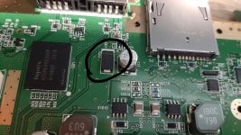
For those who've been following some of my work, I've been designing an eMMC/NAND recovery/replacement Interposer for the Wii-U. This PCB is designed to fit cleanly into place on the Wii-U mainboard without requiring the installer to remove the BGA eMMC module. This tool allows you to more easily read/dump the existing eMMC as well as serving as an eMMC replacement via MicroSD.

NAND-AID Top.jpg


The Wii-U NAND-AID is ready for public testing. Based on the feedback and data accumulated, changes will be made accordingly.

I'm going to ask of course that these not be re-uploaded or shared anywhere else. These are EVAL PCBs and aren't for public consumption. Tweaks/changes will be made based on community feedback so please document your testing in this thread. Again, this is a design in progress and the point of this public test is to resolve any issue and to put just a little more polish on the interposer.

The BOM is included within the zip file. These things are extremely cheap to make so it shouldn't cost hardly any money.

****ORDER THESE WITH A PCB THICKNESS OF EITHER 0.6MM OR 0.8MM AND INSULATE THE BOTTOM OF THE PCB****

The "DIS" jumper pulls the clock on the eNAND/eMMC to ground so that it's not floating. You'll want to keep this opened when dumping the eMMC and short it once you're finished with the original eMMC so that it has a defined logic state.

I don't have time to maintain a GITHUB for this, I just want to design this thing and get it out in the public so that people have a reasonably decent solution and answer for their NAND corrupt WIi-Us.

Thank you everyone.

EDIT: 7/14/2023

@skawo was kind enough to take the time to document the procedure of installing the NAND-AID and recovering the data. You can find that information, here.
 

Attachments

  • Wii-U NAND-AID EVAL V2.zip
    36.3 KB · Views: 78
Last edited by Voultar,

V10lator

Well-Known Member
Member
Joined
Apr 21, 2019
Messages
2,639
Trophies
1
Age
36
XP
5,501
Country
Germany
Could this be useful for a MLC-bricked Wii U?
No.... Just kidding, this has been specially made for MLC bricked Wii Us.

@Voultar I think I see a minor issue already: The solder pads for a MLC dump. You need to add a pin header, right? One facing up wouldn't fit under the RF case and one facing to the side would either crash with the SD slot or the... 330 thing on the Wii Us motherboard. So one would have to solder a (up facing) pin header to the QSB, solder the QSB in, do the dump, desolder the QSB, desolder the pin header and re-solder the QSB.

//EDIT: Also at the old thread you told to add a .1uF capacitor ( to the two pads right below the card reader, right?). Is this 0.1uF or 1uF ? Cause when googling this I find different answers, ranging from 0.1 to 1... ^^
 

Voultar

Well-Known Member
OP
Newcomer
Joined
Nov 1, 2021
Messages
59
Trophies
0
Age
44
XP
322
Country
United States
No.... Just kidding, this has been specially made for MLC bricked Wii Us.

@Voultar I think I see a minor issue already: The solder pads for a MLC dump. You need to add a pin header, right? One facing up wouldn't fit under the RF case and one facing to the side would either crash with the SD slot or the... 330 thing on the Wii Us motherboard. So one would have to solder a (up facing) pin header to the QSB, solder the QSB in, do the dump, desolder the QSB, desolder the pin header and re-solder the QSB.

You don't need to add a pin header. You can solder directly to these PTHs and be perfectly fine. I actually don't advise installing a dupont header here.

I wanted to put an FFC interconnect but I felt that it would make it too proprietary. With these, people can use whatever they have to make a dump of their Wii-U's NAND. Seeing that this only really needs to be done once, I don't see the point of populating a header on the PCB, other than for testing/debugging purposes which won't be the general use-case for this.

//EDIT: Also at the old thread you told to add a .1uF capacitor ( to the two pads right below the card reader, right?). Is this 0.1uF or 1uF ? Cause when googling this I find different answers, ranging from 0.1 to 1... ^^

- .1uF is probably sufficient to debounce the SD card in this particular environment. Honestly, anything between 100nF to 10uF should be just fine.
 
  • Like
Reactions: eyeliner

V10lator

Well-Known Member
Member
Joined
Apr 21, 2019
Messages
2,639
Trophies
1
Age
36
XP
5,501
Country
Germany
You don't need to add a pin header. You can solder directly to these PTHs and be perfectly fine.
Ah, so the holes in the middle of these pads are just IVs and not meaned for a pin header?

Also have a look at my last EDIT, please. I wrote it while you posted your answer so a high chance you overlooked it.

//EDIT: Or is this uF thing, as a friend of me (who is engineer at frauenhofer institute) likes to say, "not that important" and anything between 0.1 and 1uF will work?
 

Voultar

Well-Known Member
OP
Newcomer
Joined
Nov 1, 2021
Messages
59
Trophies
0
Age
44
XP
322
Country
United States
Ah, so the holes in the middle of these pads are just IVs and not meaned for a pin header?

Developers (me and other people) may populate a pin header on there and keep the RF plating off if we're constantly dumping/writing to the eMMC. But 99% of the people who are just looking to get their Wii-U working again won't be doing this. They'll be doing a 1 time read/dump of their EMMC and using that to rescontruct/rebuild their MLC onto a MicroSD card.

It's provisioned for a pin-header, but that's not for a general installation and mainly for debugging/working with the onboard eNAND.
 
  • Like
Reactions: eyeliner

V10lator

Well-Known Member
Member
Joined
Apr 21, 2019
Messages
2,639
Trophies
1
Age
36
XP
5,501
Country
Germany
It's provisioned for a pin-header
Did you check if it still fits with a pin header added? Cause the pins will look around 0.5 to 1mm out of the holes at the lower side. Again: This is just minor issue talk cause it's just for devs like you and me, not for the average Joe.

Also don't ignore my question about the capacity of the capacitor, please. :(
 

Voultar

Well-Known Member
OP
Newcomer
Joined
Nov 1, 2021
Messages
59
Trophies
0
Age
44
XP
322
Country
United States
Did you check if it still fits with a pin header added? Cause the pins will look around 0.5 to 1mm out of the holes at the lower side. Again: This is just minor issue talk cause it's just for devs like you and me, not for the average Joe.

Also don't ignore my question about the capacity of the capacitor, please. :(

You cut the pins flush on the underside, and then apply kapton tape or some other insulator to the bottom. A 2.54mm header will not clear the RF shield. It must be kept off. You might be able to sneak in a 90 degree header, though.

I answered your capacitor question, several posts ago. I don't want to repeat myself a thousand times. Sorry.
 

Lazr1026

Well-Known Member
Member
Joined
Oct 30, 2020
Messages
124
Trophies
0
Age
17
XP
730
Country
United States
oh yeah, i recently got a retail hynix that has these (my kiosk has it too but im not worried about that)
 

Attachments

  • 20230408_100138.jpg
    20230408_100138.jpg
    2.3 MB · Views: 111

Voultar

Well-Known Member
OP
Newcomer
Joined
Nov 1, 2021
Messages
59
Trophies
0
Age
44
XP
322
Country
United States
oh yeah, i recently got a retail hynix that has these (my kiosk has it too but im not worried about that)

That is just an extra decoupling capacitor that stacks in parallel with the electrolytic capacitor directly to its right.

It can be removed with no consequence. Nintendo dropped it.
 

Lazr1026

Well-Known Member
Member
Joined
Oct 30, 2020
Messages
124
Trophies
0
Age
17
XP
730
Country
United States
That is just an extra decoupling capacitor that stacks in parallel with the electrolytic capacitor directly to its right.

It can be removed with no consequence. Nintendo dropped it.
im aware they dropped it. 2/7 of my consoles have it
 

SDIO

Well-Known Member
Member
Joined
Feb 13, 2023
Messages
2,266
Trophies
0
Age
28
XP
1,384
Country
Germany
JLCPCB gives me the option to get tented VIAs. Can you say what would happend to the vias for the PIN header?
Maybe it would be better to have SM Pads instead of the THs. Then one could juse order the PCBs with tended vias and has no risk of shorting anything out.
I also don't plan to fit a header there and will solder the wires directly.
Post automatically merged:

Also you said either to use 0.6mm or 0.8, which one would be the prefereded one if I can choose between them?
Post automatically merged:

You also had this SD adapte rfor using a cardreader to dump it. Maybe you want to share the gerbers for that here too?
 
Last edited by SDIO,

Voultar

Well-Known Member
OP
Newcomer
Joined
Nov 1, 2021
Messages
59
Trophies
0
Age
44
XP
322
Country
United States
OK, I'm already going to rework this PCB based on the feedback.

The PTHs are gone. I've buried vias in pads for all of the break-out connections.

Top.png


The bottom of the board will pull the solder resist over these vias, which if the fabrication is good, will mean that you'll no longer have to insulate the bottom of the PCB.

Bottom.png


Notice that the "leg" has been removed. There's a nice large via that will allow you to grab ground form an empty capacitor footprint. This should be much easier to deal with.

The files are embedded in this post.

Also you said either to use 0.6mm or 0.8, which one would be the prefereded one if I can choose between them?

If they cost the same, .6mm will be easier to maneuver. .8mm thickness will also work fine, too.

You also had this SD adapte rfor using a cardreader to dump it. Maybe you want to share the gerbers for that here too?

Those haven't arrived yet. Once they come in and I can give them a looking over, I'll release those as well.
 
Last edited by Voultar,
  • Like
Reactions: Magnus87 and r1vver

SDIO

Well-Known Member
Member
Joined
Feb 13, 2023
Messages
2,266
Trophies
0
Age
28
XP
1,384
Country
Germany
With the new GND via I see the problem, that it is under the SD slot. So the SD Slot can only be soldered after the QSB is soldered to the board. That would be a problem if I want to sent this out to people with a pre soldered SD slot. So maybe the "leg" was better in that regard.

Do have a rough idea when the SD Adapter will arrive, so I can decide if it is worth waiting on that with the order.

EDIT: also I found it very hard to solder to GND on the Wii U board as it is really sucking the heat away so I had to preheat it with hot air. This could be very difficult with the GND via
 

V10lator

Well-Known Member
Member
Joined
Apr 21, 2019
Messages
2,639
Trophies
1
Age
36
XP
5,501
Country
Germany
With the new GND via I see the problem
Beside what you see it's also not that easy to let the solder flow through a hole. Like there will be a air bubble in that hole making it hard to let the solder pass through + you can't heat the solder pad below the hole with 0815 soldering equipment, making it more hard to create a stable contact.
 

Voultar

Well-Known Member
OP
Newcomer
Joined
Nov 1, 2021
Messages
59
Trophies
0
Age
44
XP
322
Country
United States
With the new GND via I see the problem, that it is under the SD slot. So the SD Slot can only be soldered after the QSB is soldered to the board. That would be a problem if I want to sent this out to people with a pre soldered SD slot. So maybe the "leg" was better in that regard.

Do have a rough idea when the SD Adapter will arrive, so I can decide if it is worth waiting on that with the order.

The leg can be extremely challenging to solder to as the capacitor it solders to sinks a tremendous amount of heat, even I had trouble with it.

I'll think of other grounding locations. But honestly, this MicroSD holder solders very, very quickly and easily.

If the person who's installing this can't do the very basic, 3 minutes solder rework to install the MicroSD port, they I don't believe this is something they should be doing.

Beside what you see it's also not that easy to let the solder flow through a hole. Like there will be a air bubble in that hole making it hard to let the solder pass through + you can't heat the solder pad below the hole with 0815 soldering equipment, making it more hard to create a stable contact.

That joint will be the easiest joint to solder of all soldering required. The diameter of the hole is 1.5mm, that is massive. And flooding fresh solder into the region will not create any sort of air bubble, it will wet beautifully.

I need you everyone to keep in mind that this project, regardless of the design choices that I make to simplify the procedure, is NOT meant for people with limited soldering ability. I appreciate the things you're bringing up and I'm keeping inventory of them, but ultimately this isn't going to be an activity for people who can't do surface mount work such as this. I hope you understand.
 

V10lator

Well-Known Member
Member
Joined
Apr 21, 2019
Messages
2,639
Trophies
1
Age
36
XP
5,501
Country
Germany
I'll think of other grounding locations.
Maybe make it a cable (like VCC) ?
If the person who's installing this can't do the very basic, 3 minutes solder rework to install the MicroSD port, they I don't believe this is something they should be doing.
That's where we think differently. A soldering n00b might have a hard time to solder the small contacts of the data lines but why make it even more hard with more micro soldering while there are people willing to give away your PCB design with the SD slot attached already?
 
  • Like
Reactions: sergio_prado

Voultar

Well-Known Member
OP
Newcomer
Joined
Nov 1, 2021
Messages
59
Trophies
0
Age
44
XP
322
Country
United States
why make it even more hard with more micro soldering while there are people willing to give away your PCB design with the SD slot attached already?

I understand what you're saying. But also understand that I don't have a lot of free-time to constantly rework a PCB that I'm designing for free just to spare someone the 3 minutes it would take to install it.

I welcome all feedback and will weigh what I feel is worth investing time into and discarding what I feel isn't incredibly important.
 
  • Like
Reactions: nikeymikey

Site & Scene News

Popular threads in this forum

General chit-chat
Help Users
    Purple_Heart @ Purple_Heart: ye