Tutorial
Updated
My Experience Installing an OLED Permanent DAT0/CMD/CLK Breakout PCB (EMMC reball) SUCCESSFULLY as a Beginner: a Guide of Sorts
Update: Don't follow this guide. I thought my install worked because I was using my switch as normal (Iplayed many hours of TOTK with it) after I installed the adapter for over a week while I waited for the modchip to come in from China. Since I have installed the modchip, I cannot boot OFW or EMUMMC, and I keep getting EMMC errors and problems. I am afraid I damaged the EMMC during the adapter installation, I am ordering a blank EMMC to see if I can fix the switch.
Disclaimer:
Before getting into this post/guide I want to say I honestly don’t really recommend this. The risk v.s. reward is skewed heavily toward risk, especially when most are having lasting success with the newer 4 point DAT0 adapters. It was more difficult than I expected, even as someone with many hours of soldering experience. This is just an account of what worked (and didn’t work) for me and should NOT be counted on to work for you as well. This post does not cover the installation of a modchip.
A health and safety notice:
This project uses lots of hazardous materials. Leaded solder and flux fumes are toxic, so ensure proper ventilation and wear gloves. However, of all chemicals you will be using for this, the leaded solder paste is the most dangerous. It is composed of tiny particles of lead that can AND WILL hitchhike their way into your body. Once these lead particles make it into your body, they are deposited in tissues and cannot be eliminated. I would be very cautious and conservative with this stuff.
A little background and rationale for how I ended up here:
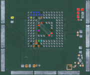
Although I have owned a switch since late 2018, I only got into the modding scene recently. A few months back I decided to put a Picofly in my switch Lite. Wow, what a difference that made! But after a few days with it, I began missing the beautiful screen and docking functionality of my OLED. However, after doing some research on OLED modding, I learned that compared to the Lite, the OLED is much jankier to mod. Two of the points on the OLED are not exposed on the circuit board. Because of this, you must scratch through the PCB to expose the CLK point and use a shim to pressure-fit a contact on the DAT0 point.
It turns out that I’m not the only one who didn’t like the jank of the OLED mod. Although this method is by far the most popular way to mod the OLED, two other more permanent (yet riskier) ways exist. The first still uses the scratch method to expose the CLK point, but instead of pressure fitting a DAT0 point, a tiny ~50 gauge wire is soldered to the DAT0 ball under the EMMC, requiring the EMMC to be desoldered and re-balled. The EMMC is a sensitive component, and desoldering it is risky business. It holds the keys to the system and without it, the switch will be essentially bricked, with the only fix being very complicated and still results in a soft ban for life. The second method, which I am covering in this post, uses a PCB between the EMMC and the main motherboard to break out the difficult to solder points. It still requires hot air rework and risks the EMMC, but doesn’t require scratching the PCB to expose the CLK point. Out of all the ways to install a modchip in a switch OLED, this is by far the cleanest and longest lasting method. Although I had never done BGA work in the past, I figured this would be a great reason to learn.
The tools and supplies:
In order to do BGA rework, I needed a few tools that I did not have. Money is a little tight for me at the moment, so I had to find the most affordable tools that would get the job done. Below is a list of all the tools I used on this project, where I got them, and how much they cost shipped to me (in Feb 2024).
A side note on preheaters:
During my research I found many conflicting reports on the need of an IR preheater to preheat the board for desoldering the EMMC. I did order a preheater, but I had to return it because they sent me the 240v EU version, even though I ordered the 110v US version. Instead, I used a heatgun to preheat the board which worked just fine.
Total cost of tools and supplies: $201
The breakout adapters are the only part of this build that you can’t just buy from Amazon or AliExpress. From my understanding, a version used to come with later revisions of the HWFLY, but those are no longer around. A Malaysian website still has them for sale under the title “HWFLY EmmC Dat0 Pcb (Reball Emmc Adapter)” but they don’t seem to ship to the United States. If anyone has any experience with these from this source, please comment about it!
The method I chose was to have them made by JLPCB. A github file by abal1000x titled emmc_adapter v2.0.0 revision is available. You can download the gerber.zip from this file and upload it JLPCB. The only setting you change is the PCB thickness to 0.6mm. You can then place your order. I only ordered 5, thinking it would be plenty. Thank god they sent me 35, because I ended up burning through quite a few of them with practice and failed attempts. My suggestion would be to order 20 or 30 minimum so you can have some to practice on and some for failed attempts. Additionally, the quality of these is ok, but not the greatest. If you use a solder wick on these more than about once (sometimes even once is too much) you will start exposing traces and the pcb is toast. I wonder if other PCB prototype manufacturers would make better quality boards. Again comment if you have any suggestions!
Now for the practice:
It would have been smart of me to practice working with some ram chips from junk boards before moving onto a switch but I got excited and didn’t do that. However, I did practice reballing on some the pcb breakouts before moving to the actual switch though. The video “You CAN Easily Reball An EMMC Chip! (Nintendo Switch, Flash Drive, Wii U)” by chase fornier on YouTube shows pretty well the process of reballing, however I would dry out your solder paste between some paper towels to avoid the bubbles he got. Additionally, as I am writing this, I found a practice set on AliExpress titled “bga practice BGA chip BGA153 welding machine practice planting ball and tin practice chip steel mesh board set.” Its only $7 and is the same EMMC that the switch uses, so that might be worth a shot too.
To practice, I first prepped a few PCB breakouts with flux and ran a big bead of leaded solder across the solder pads with a flat tip on my soldering iron set to 350C. Then I used about a quarter inch length of soldering wick and flux to suck up the excess solder and flatten the tinned pads. Be careful with the solder wick, it is abrasive and will expose traces PCB adapters. After that, I cleaned the chip with isopropyl alcohol and taped it down with Kapton tape to a silicon pad I had underneath my microscope, leaving the BGA array exposed. I lined up my stencil and spread some paper-towel-dried solder paste over the stencil with a razor blade. I scraped away the excess and repeated this until all holes in the stencil were well filled. I then carefully used my tweezers to hold down the stencil and remove my other hand to grab the hot air nozzle. Using the hot air at 350C with the 6mm tip I melted the solder paste in the stencil. I continued to hold the stencil until the solder had hardened. I then gently pried the chip off of the stencil. To center up all the balls I ran the hot air back over the reballed chip and remelted the balls. If the stencil moved slightly during the process, this will center things up.
After I had a few reballed chips, I decided to practice soldering them together. I would take a regular chip that had no balls on it, tape it down, put some flux on the solder pads, and center up a reballed chip on top of it. I would then hit it with the same temp heat from the rework station, making sure to move the heat over the whole chip and wait for it to move into place. Once I saw it move I would BARELY touch it to see if it would move and snap back into place. If so, I would keep heating it for about 10-15 more seconds, tap it lightly once more and begin backing off the heat. You want to let these things cool slowly to avoid thermal stress.
One note for those more patient and smarter than I:
Because the EMMC holds the keys to the system, and heat can kill it, it would be prudent to back up the EMMC before hitting it with hot air, especially if you have the more fragile SK hynix EMMC. To do that, you would need to install a modchip the traditional way, boot to Hekate, and make a complete backup of the EMMC. That way, if the EMMC is damaged during this process, you can still install a new EMMC (they’re like $12 on aliexpress) and restore it. I did not do this, but it’s something to think about.
The real deal:
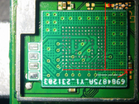
Once I felt comfortable from my practice runs, I decided to move to a switch. I took out the motherboard and exposed the EMMC. At this point you should take a few pictures through the microscope, documenting the position of the chip, the markings on the motherboard that will guide you when replacing the chip, and the resistors around it that can easily become dislodged during the process. The EMMC is soldered on from the factory with lead-free solder, which is not as easy to work with as leaded solder. The temperature required to free the EMMC with unleaded solder is very close to the temperature that will damage the EMMC. Sthetix on YouTube has a video titled “CLONING AND REPLACING THE EMMC CHIP USING THE UFI BOX” which shows a good technique to heat up the chip in a stepwise fashion to desolder it. Personally, I modified this method a bit.
My method was first putting flux at the edges of the chip. Then I set my heatgun to heat level 5 of 7 and medium fan speed and heated the whole board as evenly as I could, starting far away and slowly getting closer. When the flux started to smoke, I used my other hand to get the hot air rework wand set to 350C. I double fisted the hot air gun and the rework wand for maybe 15 seconds before I put the heatgun down and grabbed my tweezers. I’d lightly tap the EMMC occasionally while working the rework wand over the chip. Of the two EMMCs I’ve done so far, one let go at 350C, another let go at 400C. If you must turn it up, do it but be cautious. Also don’t force the EMMC off the board. Make sure ALL of the balls have liquified, or you risk pulling off solder pads, and then its game over.
Once you’ve got the EMMC off, you have to reball it. I used the same method described above in the practice section to reball the breakout PCBs. After you reball the EMMC, you have to prep and reball a breakout PCB on the bottom side as well. Once you have reballed both of these and have inspected them under the microscope for uniformity and consistency of the reball job, you can move onto final prep for install.
The PCBs I got from JLPCB had ridges on the sides from manufacturing that touched resistors next to the EMMC and got in the way. Also, positioning of all the PCB adapter is critical, and with the poor tolerances from manufacturing, you can’t clearly see the positioning marks on the motherboard for proper positioning. I had to file the PCB down to the exact size of the EMMC to get it right. I put a file on my workbench and held the PCB between my index finger and thumb and lightly filed down the 3 sides without the breakout solder pads until white line was almost gone. I then cleaned the PCB adapter with isopropyl alcohol and applied a liberal dab of flux to the balls.
I cleaned the motherboard with isopropyl alcohol, let it dry, and placed the breakout PCB adapter as close to position as I could. I then put it under the microscope and nuged it into place, each corner occupying a portion of the gold markings. Then I hit it with 350C from the rework station. I continued to monitor position under the microscope while heating. When the balls on the adapter were getting close to liquifying a surge or flux came out from under the chip, and the chip moved very slightly to fully center up. I then nudged it VERY slightly to check to see if it bounced back and recentered. I kept heating it for about another 15 seconds after that to ensure all the balls had melted. I then slowly backed off the rework wand, continuing to hit it with air, so I could cool it down slowly and not risk the joints cracking from thermal stress. After this I repeated the process for the EMMC.
Checking your work:
After you have finished the BGA work, you need to ensure you have done it right before you assemble it and put power to it. This is where the multimeter comes in. First clean the chip and area with isopropyl alcohol and a toothbrush. Then set your multimeter to diode mode and place the negative (black) to ground, the EMMC shield can be used as a ground. The CLK, DAT0, and CMD points, which are the 3 pads closest to the small shoulder/notch should read around 0.750 (+/- 0.150). The VDDF point which is the pad closest to the large shoulder/notch should not read in this orientation. Then, switch the positive (red) to touch the ground and use the negative to probe the pads. The CLK, DAT0, and CMD points should read around 0.450 in this position and the VDDF should read around 0.400. If all checks out, you are good to try and power it on. To power it on for testing you just need to connect the screen ribbon cable, the ribbon cable below the fan for the power button, and the battery.
Troubleshooting:
If all your readings check out on the multimeter but you’re not getting the device to power on at all, then you likely need to reflow your work. If that doesn’t work, I’d redo the reball job. If you are not getting readings, or are getting the wrong readings while checking your work with the multimeter, it is likely that EMMC is not positioned right. It is extremely easy to mess up the positioning of these things. I did on my first attempt, and didn’t even realize it till I couldn’t get a reading on the multimeter, and checked it again under the scope.
Disclaimer:
Before getting into this post/guide I want to say I honestly don’t really recommend this. The risk v.s. reward is skewed heavily toward risk, especially when most are having lasting success with the newer 4 point DAT0 adapters. It was more difficult than I expected, even as someone with many hours of soldering experience. This is just an account of what worked (and didn’t work) for me and should NOT be counted on to work for you as well. This post does not cover the installation of a modchip.
A health and safety notice:
This project uses lots of hazardous materials. Leaded solder and flux fumes are toxic, so ensure proper ventilation and wear gloves. However, of all chemicals you will be using for this, the leaded solder paste is the most dangerous. It is composed of tiny particles of lead that can AND WILL hitchhike their way into your body. Once these lead particles make it into your body, they are deposited in tissues and cannot be eliminated. I would be very cautious and conservative with this stuff.
A little background and rationale for how I ended up here:
Although I have owned a switch since late 2018, I only got into the modding scene recently. A few months back I decided to put a Picofly in my switch Lite. Wow, what a difference that made! But after a few days with it, I began missing the beautiful screen and docking functionality of my OLED. However, after doing some research on OLED modding, I learned that compared to the Lite, the OLED is much jankier to mod. Two of the points on the OLED are not exposed on the circuit board. Because of this, you must scratch through the PCB to expose the CLK point and use a shim to pressure-fit a contact on the DAT0 point.
It turns out that I’m not the only one who didn’t like the jank of the OLED mod. Although this method is by far the most popular way to mod the OLED, two other more permanent (yet riskier) ways exist. The first still uses the scratch method to expose the CLK point, but instead of pressure fitting a DAT0 point, a tiny ~50 gauge wire is soldered to the DAT0 ball under the EMMC, requiring the EMMC to be desoldered and re-balled. The EMMC is a sensitive component, and desoldering it is risky business. It holds the keys to the system and without it, the switch will be essentially bricked, with the only fix being very complicated and still results in a soft ban for life. The second method, which I am covering in this post, uses a PCB between the EMMC and the main motherboard to break out the difficult to solder points. It still requires hot air rework and risks the EMMC, but doesn’t require scratching the PCB to expose the CLK point. Out of all the ways to install a modchip in a switch OLED, this is by far the cleanest and longest lasting method. Although I had never done BGA work in the past, I figured this would be a great reason to learn.
The tools and supplies:
In order to do BGA rework, I needed a few tools that I did not have. Money is a little tight for me at the moment, so I had to find the most affordable tools that would get the job done. Below is a list of all the tools I used on this project, where I got them, and how much they cost shipped to me (in Feb 2024).
A side note on preheaters:
During my research I found many conflicting reports on the need of an IR preheater to preheat the board for desoldering the EMMC. I did order a preheater, but I had to return it because they sent me the 240v EU version, even though I ordered the 110v US version. Instead, I used a heatgun to preheat the board which worked just fine.
| Hot air station/ soldering iron | Silverflo 8586D | AliExpress | $59 | Way better than I expected. Did the job. |
| Heat gun | Bauer 1600 watt | Harbor Freight | $40 | Had this for a few years. Decent gun. |
| Digital Microscope | “5.5 Inch LCD Digital Microscope 1000X…” | AliExpress | $33 | OK for $33 this thing rocks! Can’t believe I did my Lite without this. |
| Multimeter with Diode mode | 7 function multimeter | Harbor freight | $5 | It works |
| Re-balling Stencil | Amaoe EMMC:3 Stencil | AliExpress | $3 | Ehh, it worked. If you can shell out for a magnetic stencil and holder from the same brand, I’d do that. Not sure if it would hold the pcb tho. |
| Solder Paste | Mechanic XGZ40 | AliExpress | $4 | Seems like decent stuff, I have nothing to compare it to. |
| Kapton Tape | 50mmx33M | AliExpress | $10 | Kapton tape is Kapton tape. |
| Flat soldering Iron Tips | 900M-T-4C | Amazon | $10 | Bought this 5-pack years ago. They work well and last a while. |
| Flux | MG-Chemicals 8341 | Amazon | $17 | Expensive, but good shit. |
| solder wick | I used 1.5mm, but I think 1mm might work better. | $5? | Not much to say here, don’t know the brand I used. | |
| Leaded solder | 60Sn/40Pb or close should work | $10? | Buy good stuff, I’ve cheaped out in the past and regretted it. | |
| PCB Breakout adapters | Design by abal1000x | JLPCB | $5 | More info below |
Total cost of tools and supplies: $201
The breakout adapters are the only part of this build that you can’t just buy from Amazon or AliExpress. From my understanding, a version used to come with later revisions of the HWFLY, but those are no longer around. A Malaysian website still has them for sale under the title “HWFLY EmmC Dat0 Pcb (Reball Emmc Adapter)” but they don’t seem to ship to the United States. If anyone has any experience with these from this source, please comment about it!
The method I chose was to have them made by JLPCB. A github file by abal1000x titled emmc_adapter v2.0.0 revision is available. You can download the gerber.zip from this file and upload it JLPCB. The only setting you change is the PCB thickness to 0.6mm. You can then place your order. I only ordered 5, thinking it would be plenty. Thank god they sent me 35, because I ended up burning through quite a few of them with practice and failed attempts. My suggestion would be to order 20 or 30 minimum so you can have some to practice on and some for failed attempts. Additionally, the quality of these is ok, but not the greatest. If you use a solder wick on these more than about once (sometimes even once is too much) you will start exposing traces and the pcb is toast. I wonder if other PCB prototype manufacturers would make better quality boards. Again comment if you have any suggestions!
Now for the practice:
It would have been smart of me to practice working with some ram chips from junk boards before moving onto a switch but I got excited and didn’t do that. However, I did practice reballing on some the pcb breakouts before moving to the actual switch though. The video “You CAN Easily Reball An EMMC Chip! (Nintendo Switch, Flash Drive, Wii U)” by chase fornier on YouTube shows pretty well the process of reballing, however I would dry out your solder paste between some paper towels to avoid the bubbles he got. Additionally, as I am writing this, I found a practice set on AliExpress titled “bga practice BGA chip BGA153 welding machine practice planting ball and tin practice chip steel mesh board set.” Its only $7 and is the same EMMC that the switch uses, so that might be worth a shot too.
To practice, I first prepped a few PCB breakouts with flux and ran a big bead of leaded solder across the solder pads with a flat tip on my soldering iron set to 350C. Then I used about a quarter inch length of soldering wick and flux to suck up the excess solder and flatten the tinned pads. Be careful with the solder wick, it is abrasive and will expose traces PCB adapters. After that, I cleaned the chip with isopropyl alcohol and taped it down with Kapton tape to a silicon pad I had underneath my microscope, leaving the BGA array exposed. I lined up my stencil and spread some paper-towel-dried solder paste over the stencil with a razor blade. I scraped away the excess and repeated this until all holes in the stencil were well filled. I then carefully used my tweezers to hold down the stencil and remove my other hand to grab the hot air nozzle. Using the hot air at 350C with the 6mm tip I melted the solder paste in the stencil. I continued to hold the stencil until the solder had hardened. I then gently pried the chip off of the stencil. To center up all the balls I ran the hot air back over the reballed chip and remelted the balls. If the stencil moved slightly during the process, this will center things up.
After I had a few reballed chips, I decided to practice soldering them together. I would take a regular chip that had no balls on it, tape it down, put some flux on the solder pads, and center up a reballed chip on top of it. I would then hit it with the same temp heat from the rework station, making sure to move the heat over the whole chip and wait for it to move into place. Once I saw it move I would BARELY touch it to see if it would move and snap back into place. If so, I would keep heating it for about 10-15 more seconds, tap it lightly once more and begin backing off the heat. You want to let these things cool slowly to avoid thermal stress.
One note for those more patient and smarter than I:
Because the EMMC holds the keys to the system, and heat can kill it, it would be prudent to back up the EMMC before hitting it with hot air, especially if you have the more fragile SK hynix EMMC. To do that, you would need to install a modchip the traditional way, boot to Hekate, and make a complete backup of the EMMC. That way, if the EMMC is damaged during this process, you can still install a new EMMC (they’re like $12 on aliexpress) and restore it. I did not do this, but it’s something to think about.
The real deal:
Once I felt comfortable from my practice runs, I decided to move to a switch. I took out the motherboard and exposed the EMMC. At this point you should take a few pictures through the microscope, documenting the position of the chip, the markings on the motherboard that will guide you when replacing the chip, and the resistors around it that can easily become dislodged during the process. The EMMC is soldered on from the factory with lead-free solder, which is not as easy to work with as leaded solder. The temperature required to free the EMMC with unleaded solder is very close to the temperature that will damage the EMMC. Sthetix on YouTube has a video titled “CLONING AND REPLACING THE EMMC CHIP USING THE UFI BOX” which shows a good technique to heat up the chip in a stepwise fashion to desolder it. Personally, I modified this method a bit.
My method was first putting flux at the edges of the chip. Then I set my heatgun to heat level 5 of 7 and medium fan speed and heated the whole board as evenly as I could, starting far away and slowly getting closer. When the flux started to smoke, I used my other hand to get the hot air rework wand set to 350C. I double fisted the hot air gun and the rework wand for maybe 15 seconds before I put the heatgun down and grabbed my tweezers. I’d lightly tap the EMMC occasionally while working the rework wand over the chip. Of the two EMMCs I’ve done so far, one let go at 350C, another let go at 400C. If you must turn it up, do it but be cautious. Also don’t force the EMMC off the board. Make sure ALL of the balls have liquified, or you risk pulling off solder pads, and then its game over.
Once you’ve got the EMMC off, you have to reball it. I used the same method described above in the practice section to reball the breakout PCBs. After you reball the EMMC, you have to prep and reball a breakout PCB on the bottom side as well. Once you have reballed both of these and have inspected them under the microscope for uniformity and consistency of the reball job, you can move onto final prep for install.
The PCBs I got from JLPCB had ridges on the sides from manufacturing that touched resistors next to the EMMC and got in the way. Also, positioning of all the PCB adapter is critical, and with the poor tolerances from manufacturing, you can’t clearly see the positioning marks on the motherboard for proper positioning. I had to file the PCB down to the exact size of the EMMC to get it right. I put a file on my workbench and held the PCB between my index finger and thumb and lightly filed down the 3 sides without the breakout solder pads until white line was almost gone. I then cleaned the PCB adapter with isopropyl alcohol and applied a liberal dab of flux to the balls.
I cleaned the motherboard with isopropyl alcohol, let it dry, and placed the breakout PCB adapter as close to position as I could. I then put it under the microscope and nuged it into place, each corner occupying a portion of the gold markings. Then I hit it with 350C from the rework station. I continued to monitor position under the microscope while heating. When the balls on the adapter were getting close to liquifying a surge or flux came out from under the chip, and the chip moved very slightly to fully center up. I then nudged it VERY slightly to check to see if it bounced back and recentered. I kept heating it for about another 15 seconds after that to ensure all the balls had melted. I then slowly backed off the rework wand, continuing to hit it with air, so I could cool it down slowly and not risk the joints cracking from thermal stress. After this I repeated the process for the EMMC.
Checking your work:
After you have finished the BGA work, you need to ensure you have done it right before you assemble it and put power to it. This is where the multimeter comes in. First clean the chip and area with isopropyl alcohol and a toothbrush. Then set your multimeter to diode mode and place the negative (black) to ground, the EMMC shield can be used as a ground. The CLK, DAT0, and CMD points, which are the 3 pads closest to the small shoulder/notch should read around 0.750 (+/- 0.150). The VDDF point which is the pad closest to the large shoulder/notch should not read in this orientation. Then, switch the positive (red) to touch the ground and use the negative to probe the pads. The CLK, DAT0, and CMD points should read around 0.450 in this position and the VDDF should read around 0.400. If all checks out, you are good to try and power it on. To power it on for testing you just need to connect the screen ribbon cable, the ribbon cable below the fan for the power button, and the battery.
Troubleshooting:
If all your readings check out on the multimeter but you’re not getting the device to power on at all, then you likely need to reflow your work. If that doesn’t work, I’d redo the reball job. If you are not getting readings, or are getting the wrong readings while checking your work with the multimeter, it is likely that EMMC is not positioned right. It is extremely easy to mess up the positioning of these things. I did on my first attempt, and didn’t even realize it till I couldn’t get a reading on the multimeter, and checked it again under the scope.
Last edited by ratgoul,