So I was looking at the delayered images of the Switch Lite PCB here:
http://balika011.hu/switch/lite/
If you remove the first layer, you get this view:
And if you remove 2 more layers you can see this:
So to me it seems, that the first layer, is connected to 19 points on the third layer.
If we translate these pins to the top layer, we can see which of these points are connected:
So I had a bit of free time and doodled a QSB, which is looks something like this:
The idea goes like this:
1) Remove the eMMC and clean it
2) Clean the Switch PCB
3) Solder the QSB to the 19 points on the Switch PCB
4) Use thin double sided tape and apply it to the Switch PCB
5) Flip over the eMMC, so the BGA points upwards and place it face down on the double sided tape
6) Bend the QSB over towards the BGA
7) Solder the QSB onto the BGA and restore the connection to the Switch PCB this way
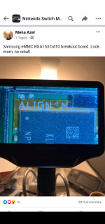
8) Use exposed DAT0 to solder it to the modchip
So if you'd look at it from the side, it would look like this:
NOTE: The design has a few errors on the bottom part - I mirrored it incorrectly and the pin on the bottom needs to be rerouted to the corresponding pin on the BGA.
I just couldn't be assed to finish it 100% in Paint.net, but you should get the idea

As I said, this is just me talking out of my ass, but should it be possible to create such a QSB, then I'm sure that this will be a lot easier to install.
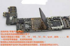
Because reworking a BGA, even that small, is not as easy as it seems - but removing the eMMC, cleaning it and soldering 19-20 pins on both sides should be as hard/easy as soldering the SoC QSB.
What do you guys think?