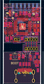
Introducing the Mcfly, a barebones RP2040 board designed from the ground up to be compact, simple and slim. With a USB port that breaks away after initial programming the overall thickness of the board can be reduced to ~2mm. An X and Y footprint of ~19x19mm makes this stripped back board suitable for internal installation in the switch. No stone was left unturned in the design of this board, with all the features of a conventional picofly install present including the debug WS2812 LED and the jumper to reset the glitch timings as well as the inclusion of a 6 pin fpc connector designed to be used with HWFLY CPU flex cables, simplifying the installation and reducing the risk of damaging the APU. Despite the breakaway connector the Mcfly can be updated too, using a 5 pin 1.27mm header the usb section can be either temporarily soldered back on, or a pin header attached and it held in place whilst the board is reprogrammed.
View attachment 360663View attachment 360665
Upon completion of testing the Mcfly will be released under the Creative Commons Attribution Share Alike licence, opening the door for design improvements and alterations by the community, as well as commercialisation by a third party, at this moment i do not plan to commercialise this design myself, I simply dont have the time to sell these personally. If you would be interested in selling these or know someone who is please get in touch! This wont be price competitive with a 2040-Zero, in low quantities that's simply not possible, nor will it be as easy to install as the inevitable HwFly picofly board. The goal is for this to be a community driven open source solution that simplifies the install to the greatest extent possible whilst still being reasonably low cost, using off the shelf parts you can get from any component retailer
View attachment 360664
As it stands the hardware layout is largely complete for now, pending feedback from testers, components have been ordered and the PCBs have also been ordered. I should recieve them in a week ish and can build a few.
I cannot make this a reality without your help, i'm currently looking for testers able to give this a go and provide feedback, my switch is an unpatched erista and i cant afford to buy another just for this project. Testers should be experienced with the switch, done several installations of other modchips and be willing to provide useful critical feedback to improve the design. If you have a HWFLY cpu cable to try with my board that would be even better as i have no idea if i've implemented that properly tbh. Please DM me if you're serious about testing this.
If you have any questions or feedback ask away!