Hacking Hardware Picofly - a HWFLY switch modchip

binkinator

Garfield’s Fitness Coach
Member
GBAtemp Patron
Joined
Mar 29, 2021
Messages
6,511
Trophies
2
XP
6,155
Country
United States
0.45mm on my oled one

Interesting…the one I put in my regular V2 Mariko comes in at .28mm

image.jpg
 

binkinator

Garfield’s Fitness Coach
Member
GBAtemp Patron
Joined
Mar 29, 2021
Messages
6,511
Trophies
2
XP
6,155
Country
United States
that pcb deffo looks thinner

Are you suggesting there’s no governing body or quality control for grey market devices coming out of China?

1675028558117.jpeg

(ya…it definitely feels more flimsy than most PCBs I have laying around.)
 

shaunsingh0207

New Member
Newbie
Joined
Jan 28, 2023
Messages
2
Trophies
0
Age
23
XP
31
Country
United States
firmware.bin is the raw dump. Flash firmware.uf2, do a
Code:
picotool save --all
and you'll find it's identical to firmware.bin.

We don't need to decompile it if we can make it run. At that point someone could just reverse engineer it, as long as it's functioning (or use it as-is). Otherwise, you're just trying to reimplement the FPGA's functionality from scratch, and we don't have the bitstream or its source. If someone with one of these chips shares their dump AND their serial (also called unique ID) then we can move forward with this. Otherwise, there's nothing to be done, someone would have to determine exactly how the HWFLY FPGA works and write an RP2040 sketch that does the same thing.

Decompiling certainly isn't a requirement, but I'd rather not run untested (and likely old) proprietary code on my switch, the important thing is now we know that this glitch is possible with an rp2040, and in my opinion it would be easier to implement it from scratch.
The easiest way to approach it would be to create a firmware for the rp2040 based off of the pikofly mcu code, then reverse engineer and emulate the fgpa with the rpi's PIO.
 

Soggytoast111

New Member
Newbie
Joined
Oct 17, 2022
Messages
4
Trophies
0
Age
38
XP
136
Country
United States
Decompiling certainly isn't a requirement, but I'd rather not run untested (and likely old) proprietary code on my switch, the important thing is now we know that this glitch is possible with an rp2040, and in my opinion it would be easier to implement it from scratch.
The easiest way to approach it would be to create a firmware for the rp2040 based off of the pikofly mcu code, then reverse engineer and emulate the fgpa with the rpi's PIO.

The issue is that it's not really public knowledge how to sync the chip with the switch to perform the glitch with the correct timing. If it was so easy then it would have been done years ago.

That's why people are trying so hard to decrypt this dump to be disassembled - we simply don't fully understand what it's doing.
 

saladus

Well-Known Member
Newcomer
Joined
Dec 26, 2022
Messages
95
Trophies
0
Location
your router's unprotected root shell
XP
170
Country
Romania
ok so the bootloader does the decryption, from 0x2C00 until almost the end firmware.bin has max entropy so it's either compressed or encrypted, but considering it doesn't do the voltage glitching I'd assume it's the latter
Post automatically merged:

maybe we should be focusing on the uf2 instead :ha:
edit: just realized binwalk says encrypted data, not that it found an encryption program, sorry
Post automatically merged:

someone with pikofly should measure the voltage of the various pinouts on startup
someone on the other thread hooked up a logic analyzer to their hwfly but i don't think it's a massive discovery :lol:
 

Attachments

  • Final_tests-Analyze_GLTCH_SW.png
    Final_tests-Analyze_GLTCH_SW.png
    49.9 KB · Views: 91
Last edited by saladus,

thesjaakspoiler

Well-Known Member
Member
Joined
Nov 20, 2018
Messages
968
Trophies
0
Age
124
XP
1,474
Country
Afghanistan
The issue is that it's not really public knowledge how to sync the chip with the switch to perform the glitch with the correct timing. If it was so easy then it would have been done years ago.
The learning process which determines the glitch timing has been described in the Spacecraft-NX code :
https://github.com/Spacecraft-NX/firmware

Glitching something with a RP has also been described :
https://github.com/ensingerphilipp/airtag-glitch-dump-improved
All that electronic stuff is on the ribbon cable.

What the pikofly solved was how to inject alternative data without the help of a dedicated FPGA.
The raspberry-pi has all kinds of cool things on board like a dma controller and other high speed data transfers from/to it's GPIO ports. So I presume they just use the emmc clock to sync the timings.
But maybe there is even a more ingenious way to accomplish that.
 

Piorjade

Well-Known Member
Member
Joined
Nov 8, 2015
Messages
142
Trophies
0
XP
407
Country
Gambia, The
The learning process which determines the glitch timing has been described in the Spacecraft-NX code :
https://github.com/Spacecraft-NX/firmware

Glitching something with a RP has also been described :
https://github.com/ensingerphilipp/airtag-glitch-dump-improved
All that electronic stuff is on the ribbon cable.

What the pikofly solved was how to inject alternative data without the help of a dedicated FPGA.
The raspberry-pi has all kinds of cool things on board like a dma controller and other high speed data transfers from/to it's GPIO ports. So I presume they just use the emmc clock to sync the timings.
But maybe there is even a more ingenious way to accomplish that.

Time to read myself into the whole SpaceNX code and draw diagrams to understand the whole procedure lmao

Too bad that I'm too dumb to actually be able to write the FPGA part.
Nevertheless, it's actually amazing how the whole hack works and how annoying it is to install it.

EDIT:
After reading a bit I wish the devs would've documented the code a bit better lmao, lots of cryptic stuff and "magic numbers".
Anyway, I've found the following file: https://github.com/hwfly-nx/firmware/blob/master/firmware/src/glitch.c
And as far as I understood the code, the FPGA doesn't actually search for the correct offsets and pulse widths for the glitch, it just uses the given offset + pulse width and returns whether the glitch was successful or not and if not then the microcontroller resets the CPU and sends a different config and retries, am I right?
I'm just trying to learn from this whole thing here..

So my current understanding is that the FPGA uses the given pulse width + offset to start the glitch and afterwards reads data on either the DAT0 or CMD line (or both?) to see if there's a specific pattern and returns "success" or not based on what it has read, right?
 
Last edited by Piorjade,

ByteFun

Member
Newcomer
Joined
May 6, 2021
Messages
17
Trophies
0
Age
34
XP
85
Country
Russia
Time to read myself into the whole SpaceNX code and draw diagrams to understand the whole procedure lmao

Too bad that I'm too dumb to actually be able to write the FPGA part.
Nevertheless, it's actually amazing how the whole hack works and how annoying it is to install it.

EDIT:
After reading a bit I wish the devs would've documented the code a bit better lmao, lots of cryptic stuff and "magic numbers".
Anyway, I've found the following file: https://github.com/hwfly-nx/firmware/blob/master/firmware/src/glitch.c
And as far as I understood the code, the FPGA doesn't actually search for the correct offsets and pulse widths for the glitch, it just uses the given offset + pulse width and returns whether the glitch was successful or not and if not then the microcontroller resets the CPU and sends a different config and retries, am I right?
I'm just trying to learn from this whole thing here..

So my current understanding is that the FPGA uses the given pulse width + offset to start the glitch and afterwards reads data on either the DAT0 or CMD line (or both?) to see if there's a specific pattern and returns "success" or not based on what it has read, right?
I also studied this firmware before. There is a presentation of how the switch glitching. As I understand it, the success flag is a request to read a specific address from memory. The FPGA is just for eMMC r/w and mosfet control based on pulse width and offset relative to something that are passed from the microcontroller to the FPGA.
 
  • Like
Reactions: impeeza

binkinator

Garfield’s Fitness Coach
Member
GBAtemp Patron
Joined
Mar 29, 2021
Messages
6,511
Trophies
2
XP
6,155
Country
United States
I also studied this firmware before. There is a presentation of how the switch glitching. As I understand it, the success flag is a request to read a specific address from memory. The FPGA is just for eMMC r/w and mosfet control based on pulse width and offset relative to something that are passed from the microcontroller to the FPGA.
Is it this guy?

https://arxiv.org/pdf/2108.06131.pdf
 

FruithatMods

Well-Known Member
Member
Joined
Dec 16, 2018
Messages
128
Trophies
0
Age
34
XP
450
Country
Germany
ok so the bootloader does the decryption, from 0x2C00 until almost the end firmware.bin has max entropy so it's either compressed or encrypted, but considering it doesn't do the voltage glitching I'd assume it's the latter
Post automatically merged:

maybe we should be focusing on the uf2 instead :ha:
edit: just realized binwalk says encrypted data, not that it found an encryption program, sorry
Post automatically merged:


someone on the other thread hooked up a logic analyzer to their hwfly but i don't think it's a massive discovery :lol:
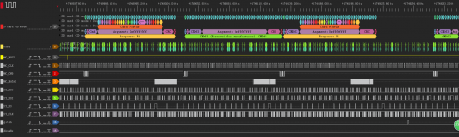
Hold on. Let's go back to this image. I think we got something here. Is it possible to get rid of all the unnecessary signals and enhance the rest?

Let's just focus on the important signals. Can we further analyse known behaviours like emmc initialisation and tag those so we can split standard signal behaviour to non standard behaviour?

I think we need to enhance!

Post automatically merged:

Is the reset line missing? Can you ask the person who analysed the signals if he also recorded the reset signal line?
Post automatically merged:

Ideally the analysis has to be taken after a factory reset to allow the HWfly to write the modified bootloader.
 
Last edited by FruithatMods,

Mansi

Well-Known Member
Newcomer
Joined
Jan 14, 2023
Messages
70
Trophies
0
Age
30
XP
331
Country
Belarus
Okay, even if the dump is partially decrypted, does anyone know how to write in C? To create firmware for rp2040.
I was thinking, what if I make a glitch without a chip, using only a programmer...
I did a full emmc dump before installing the glitch and did a re-dump after installing and got different data.
Boot1 is mostly patched. And boot2 is not touched.
I was thinking of trying to flash the patched boot1 manually and check if the console works.
And if the console turned on normally, installing the glitch would not be needed.
It would be possible to read the boot1 section as a programmer and patch it manually and everything would work.
I can throw off the files tomorrow before the installation and after the installation of the glitch.
Maybe this will help? I'm not afraid to share them, because.

I sold my console witch chip(erista). And instead I bought a (mariko) oled)))
 
  • Like
Reactions: binkinator

TheSynthax

Well-Known Member
Member
Joined
Apr 29, 2018
Messages
220
Trophies
0
XP
509
Country
United States
Okay, even if the dump is partially decrypted, does anyone know how to write in C? To create firmware for rp2040.
I was thinking, what if I make a glitch without a chip, using only a programmer...
I did a full emmc dump before installing the glitch and did a re-dump after installing and got different data.
Boot1 is mostly patched. And boot2 is not touched.
I was thinking of trying to flash the patched boot1 manually and check if the console works.
And if the console turned on normally, installing the glitch would not be needed.
It would be possible to read the boot1 section as a programmer and patch it manually and everything would work.
I can throw off the files tomorrow before the installation and after the installation of the glitch.
Maybe this will help? I'm not afraid to share them, because.

I sold my console witch chip(erista). And instead I bought a (mariko) oled)))
You can't glitch without a chip, that's what the chip does. If you write a patched bootloader without glitching the check, it will refuse to boot it. Can you share the serial of your RP2040 you took the dump from? Here's the instructions on how to do that, use the Arduino IDE method if you don't want to have to program the Pico again. https://gbatemp.net/threads/pikofly-a-probably-fake-hwfly-modchips-or-not.622701/post-10059815

At least a handful of us here know C and C++, those who do will know what to do once they're able to decrypt the binary with that serial.
 

Site & Scene News

Popular threads in this forum

General chit-chat
Help Users
    Xdqwerty @ Xdqwerty: @Purple_Heart, fuck i'm feeling old too